Optical MEMS Chemical Sensor Array

Active Publication Date: 2010-09-23
UNITED STATES OF AMERICA
View PDF7 Cites 48 Cited by
  • Summary
  • Abstract
  • Description
  • Claims
  • Application Information

AI Technical Summary

Benefits of technology

[0012]Accordingly, there remains a need for a device that has an integrated optical readout, that builds upon the prior art inventions discussed above. This device would enable multiple sensors (e.g., hundreds or more) to be interconnected on a single chip with a single input/output signal from an optical fiber. Additionally, the device would be compact, lightweight, highly selective sensor arrays with potentially hundreds of sensors on a single chip.
[0013]The disclosed MEMS sensor includes an optical readout function that relies on an on-chip integrated waveguide Fabry-Perot microcavity interferometer. Integrated waveguides enable multiple sensors to be interconnected on a single chip with a single input/output signal from an optical fiber. Consequently, th

Problems solved by technology

However, the current approaches limit the number of se

Method used


Image

  • Optical MEMS Chemical Sensor Array
  • Optical MEMS Chemical Sensor Array
  • Optical MEMS Chemical Sensor Array

Examples


Embodiment Construction

[0030]Referring now to the drawings, in which like numerals represent like elements, aspects of the exemplary embodiments will be described in connection with the drawing set.

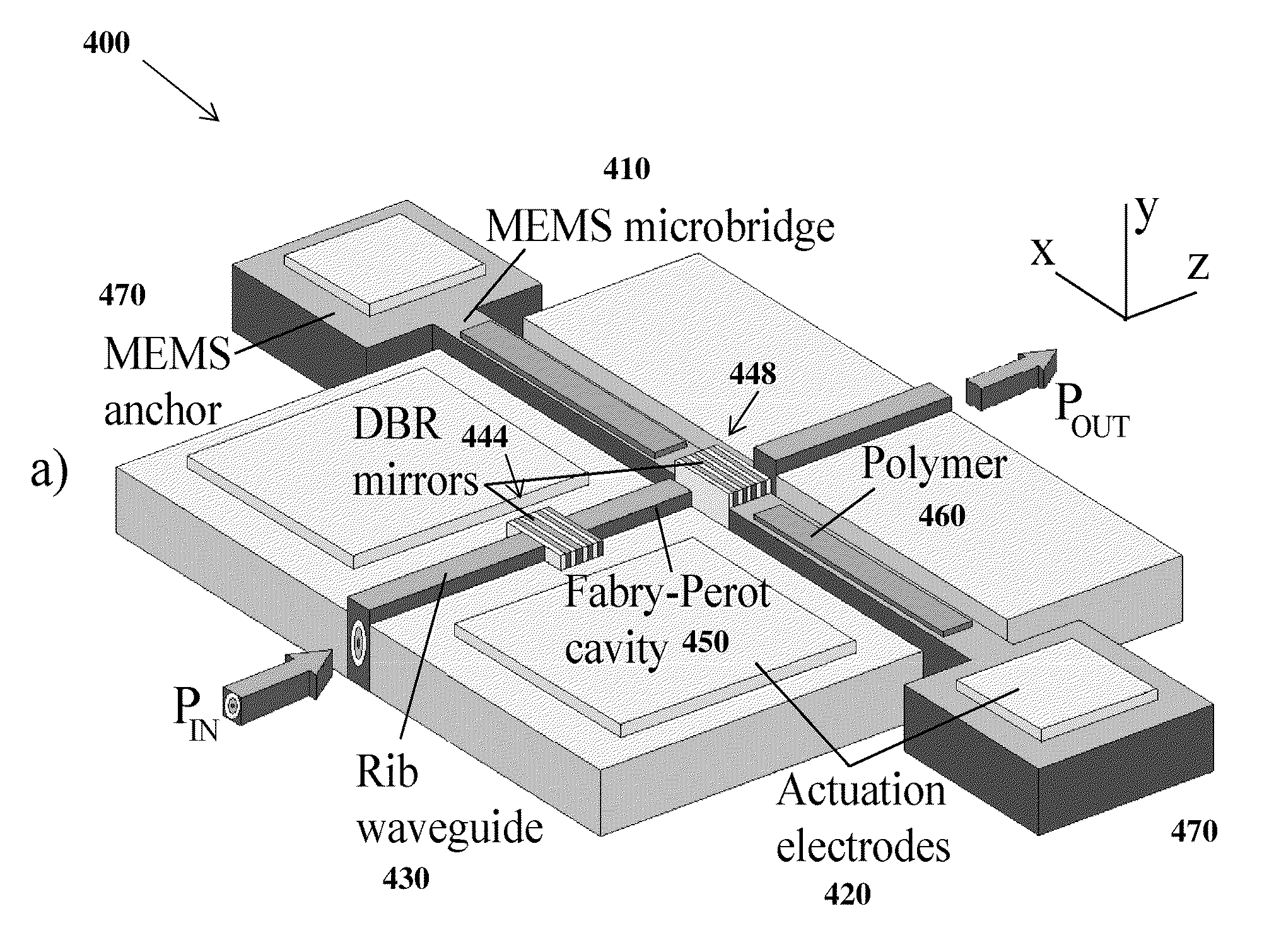
[0031]The present invention has the advantage of enabling the interconnection of many (e.g., potentially hundreds or more) sensors via integrated optical waveguides. At the same time, extremely high displacement sensitivity can be obtained via interferometry using an integrated Fabry-Perot microcavity interferometer. To take advantage of both of these features, an in-plane waveguide Fabry-Perot microcavity interferometer is utilized. One of ordinary skill in the art will understand that a Fabry-Perot microcavity interferometer can be known by other interchangeable names with the same meaning, such as Fabry-Perot microcavity, Fabry-Perot cavity; Fabry-Perot etalon cavity, Fabry-Perot optical cavity, as well as others.

[0032]FIG. 4 is a schematic of a MEMS sensor 400 in accordance with an exemplary embodiment of t...


PUM


Abstract

A change in mass of a microbridge in a mass sensor can be sensed by applying a time-varying amplitude modulated electrostatic force to excite the microbridge into resonance at the frequency of amplitude modulation. An optical energy is then transmitted at a wavelength close to a resonant wavelength of a Fabry-Perot microcavity, which is formed by etching a movable reflective mirror into a region of the microbridge and by etching a fixed reflective minor in a region spaced apart from the microbridge. The two mirrors are interconnected by an optical waveguide. The movable mirror and fixed mirror reflect the optical energy to a receiver, and a change in the Fabry-Perot microcavity's reflectivity is interferometrically determined. The change in reflectivity indicates a change in the microbridge's resonant frequency due to increased mass of the microbridge resulting from sorption of a target chemical by a layer of chemoselective material deposited on the microbridge.

Description

CROSS-REFERENCE TO RELATED APPLICATIONS[0001]This application claims priority to provisional patent application entitled, “Micro-Electro-Mechanical Chemical Sensor Array With Waveguide Interconnects and On-Chip Interferometric Optical Readout,” filed on Mar. 23, 2009, and assigned U.S. Application No. 61 / 162,373; the entire contents of which are hereby incorporated by reference.FIELD OF THE INVENTION[0002]The invention relates generally to micro-electro-mechanical systems (MEMS) based sensors. More specifically, the invention relates to a MEMS based sensor with waveguide interconnects and integrated interferometric optical readout.BACKGROUND[0003]Micro-electromechanical systems (MEMS) are micro-mechanical transducers. MEMS actuators can take an electrical signal and convert it into a mechanical signal (e.g. movement). Conversely, MEMS sensors can take a mechanical signal (e.g. displacement or frequency) and can transfer that signal to an electrical or optical carrier. MEMS chemical ...

Claims


Application Information

Patent Timeline
IPC IPC(8): G01N21/17G01B9/02
CPCG01G3/165G01N29/036G01N2291/0256G01N21/17G01B9/02051G01B2290/25G01B9/02004G01N21/75G01N2021/757
Inventor PRUESSNER, MARCEL W.STIEVATER, TODD H.RABINOVICH, WILLIAM S.
Owner UNITED STATES OF AMERICA
Why Eureka
Try Eureka