Storage element, method of manufacturing same, and semiconductor storage device

a storage element and semiconductor technology, applied in the direction of semiconductor devices, bulk negative resistance effect devices, electrical appliances, etc., can solve the problems of easy variation and inability to uniformly achieve characteristic variations, and achieve the effect of improving heat radiating properties, facilitating electric field concentration, and eliminating characteristic variations due to electric field concentration at angular parts

Active Publication Date: 2010-10-07
SONY SEMICON SOLUTIONS CORP
View PDF1 Cites 40 Cited by
  • Summary
  • Abstract
  • Description
  • Claims
  • Application Information

AI Technical Summary

Benefits of technology

[0014]In the method of manufacturing the storage element according to the above-described embodiment of the present invention, the first electrode is formed by etching back the electrode forming film and leaving the electrode forming film on the side wall of the hole such that the electrode forming film is thicker on the side of the bottom part of the hole than on the side of the opening part of the hole. In other words, the first electrode is formed so as to be thinner on the side of the opening part of the hole than on the side of the bottom part of the hole. Thus, the variable-resistance layer side of the first electrode is formed in a shape that facilitates concentration of an electric field. In addition, because the first electrode is formed as a tubular object, an electric field can be uniformly concentrated at the entire region of an upper surface part of the first electrode which part is in contact with the variable-resistance layer. Therefore, characteristic variations due to electric field concentration at angular parts can be eliminated. In addition, because the first electrode is formed by leaving the electrode forming film such that the electrode forming film is thicker on the side of the bottom part of the hole than on the side of the opening part of the hole, heat generated in the variable-resistance layer is easily radiated to the lower part side of the first electrode. That is, a heat radiating property is improved.
[0015]According to an embodiment of the present invention, there is provided a semiconductor storage device including: a select transistor composed of an insulated gate field effect transistor formed on a semiconductor substrate; an interlayer insulating film covering the select transistor formed on the semiconductor substrate; and a storage element formed on the interlayer insulating film. The storage element includes a first electrode formed on the interlayer insulating film, a second electrode formed in a position opposed to the first electrode, and a variable-resistance layer formed so as to be interposed between the first electrode and the second electrode. The first electrode is a tubular object and is formed so as to be thicker on an opposite side from the variable-resistance layer than on a side...

Problems solved by technology

A problem to be solved is that the electric field cannot be uniformly concentrated over the entire region of the part of ...

Method used


Image

  • Storage element, method of manufacturing same, and semiconductor storage device
  • Storage element, method of manufacturing same, and semiconductor storage device
  • Storage element, method of manufacturing same, and semiconductor storage device

Examples


first embodiment

1. First Embodiment

First Example of Constitution of Storage Element

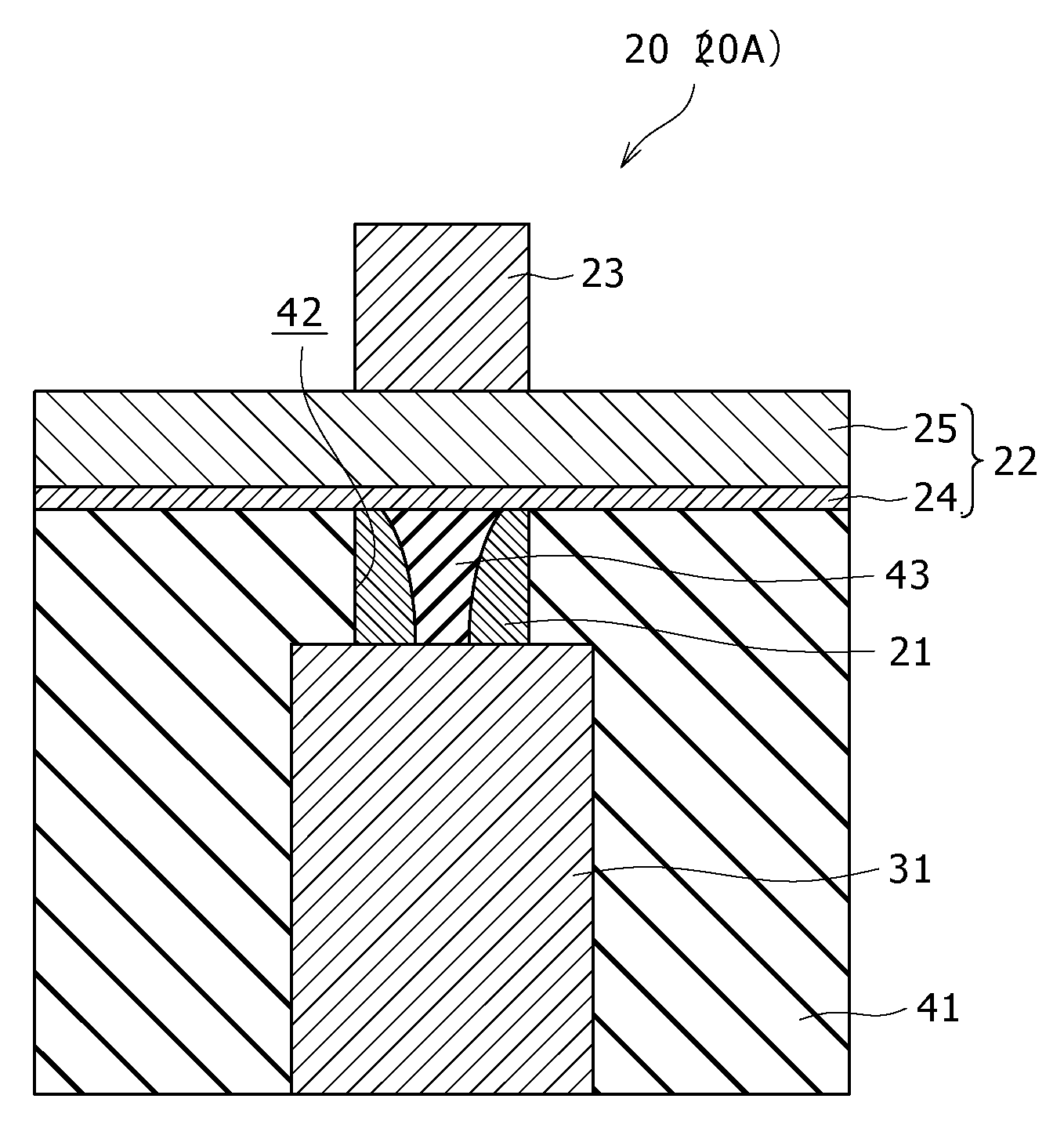
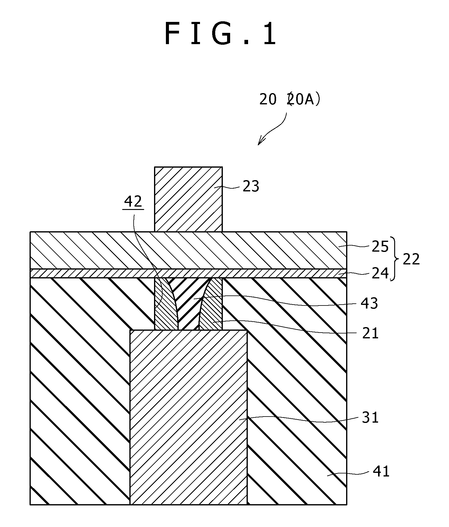
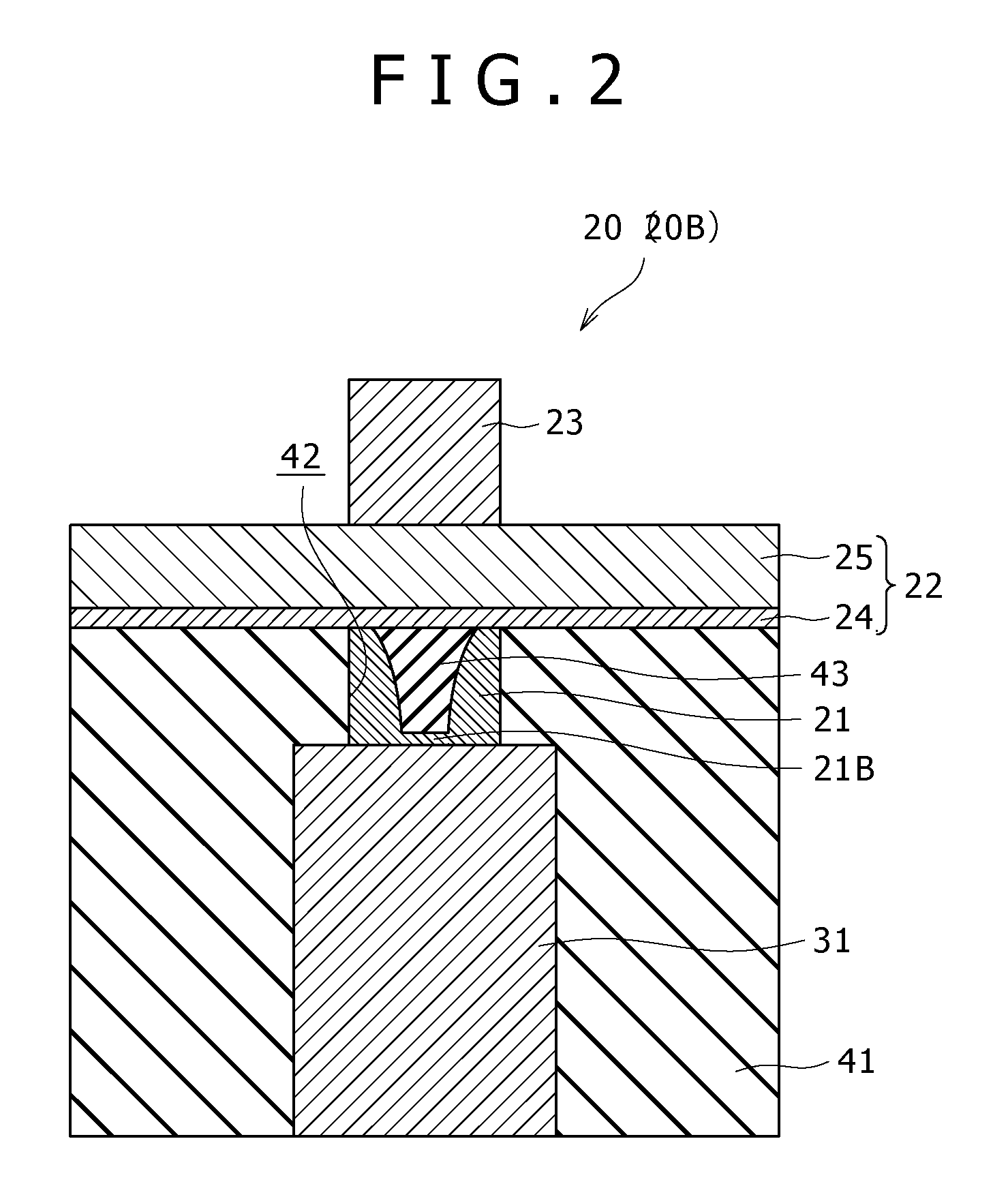
[0030]A first example of configuration of a storage element according to a first embodiment of the present invention will be described with reference to a schematic configuration sectional view of FIG. 1.

[0031]As shown in FIG. 1, a third electrode 31 is formed within an interlayer insulating film 41 on a substrate (not shown). For example tungsten nitride, titanium nitride, tungsten, titanium, gold, platinum, silver, ruthenium, tellurium or the like can be used for this third electrode 31.

[0032]The interlayer insulating film 41 is formed of a material used as an interlayer insulating film of an ordinary semiconductor device, for example. For example, a silicon oxide film, a low dielectric constant organic insulating film, a low dielectric constant inorganic insulating film or the like can be used.

[0033]A hole 42 communicating with the third electrode 31 is formed in the interlayer insulating film 41. A first electrod...

second embodiment

2. Second Embodiment

First Example of Method of Manufacturing Storage Element

[0139]A first example of a method of manufacturing a storage element according to a second embodiment of the present invention will be described with reference to schematic configuration sectional views of FIGS. 5A to 5G. The manufacturing method in the first example is an example of a manufacturing method for forming the storage element 20A described with reference to the foregoing FIG. 1.

[0140]As shown in FIG. 5A, a third electrode 31 is formed in an interlayer insulating film 41 on a substrate (not shown), and thereafter the interlayer insulating film 41 is further deposited to cover the third electrode 31. Thus, the interlayer insulating film 41 having the third electrode 31 formed in the film is formed. Then, though not shown, an etching mask is formed by resist coating, lithography techniques and the like, and a hole 42 reaching the third electrode 31 is formed in the interlayer insulating film 41 by e...

third embodiment

3. Third Embodiment

One Example of Configuration of Semiconductor Storage Device

[0169]An example of configuration of a semiconductor storage device according to a third embodiment of the present invention will be described with reference to a schematic configuration sectional view of FIG. 8 and a circuit diagram of FIG. 9.

[0170]As shown in FIG. 8, a select transistor 50 is formed on a semiconductor substrate 11. The select transistor 50 has a gate electrode 52 on the semiconductor substrate 11 with a gate insulating film 51 interposed between the semiconductor substrate 11 and the gate electrode 52. A word line W (not shown) is connected to the gate electrode 52. In addition, side walls 53 are formed on both sides of the gate electrode 52. Diffusion layers 54 and 55 serving as a source and a drain are formed in the semiconductor substrate 11 on both sides of the gate electrode 52. One diffusion layer 54 is for example connected with a first electrode 21 of a storage element 20 by a p...


PUM


Abstract

Disclosed herein is a storage element including: a first electrode; a second electrode formed in a position opposed to the first electrode; and a variable-resistance layer formed so as to be interposed between the first electrode and the second electrode. The first electrode is a tubular object, and is formed so as to be thicker on an opposite side from the variable-resistance layer than on a side of the variable-resistance layer.

Description

BACKGROUND OF THE INVENTION[0001]1. Field of the Invention[0002]The present invention relates to a storage element, a method of manufacturing the same, and a semiconductor storage device.[0003]2. Description of the Related Art[0004]Semiconductor devices including nonvolatile memory cells such as an EEPROM (Electrically Erasable and Programmable ROM), a flash memory and the like are now being used in various electronic devices. To improve reliability such as the number of times of rewriting, data retention resistance and the like of the semiconductor devices and to miniaturize the structure of the semiconductor devices are important challenges.[0005]Resistance change type memories have recently been drawing attention because of advantages thereof from viewpoints of reliability and miniaturization over flash memory structures typified by a floating type already available on the market. The resistance change type memories include ARAM, RRAM, PCRAM, MRAM, Spin RAM and the like. These re...

Claims


Application Information

Patent Timeline
IPC IPC(8): H01L45/00H01L21/02
CPCH01L45/06H01L45/1273H01L45/142H01L45/143H01L27/2436H01L45/085H01L45/1233H01L45/146H01L45/144H10B63/30H10N70/245H10N70/8418H10N70/231H10N70/8822H10N70/8825H10N70/011H10N70/826H10N70/8828H10N70/8833
Inventor SUMINO, JUN
Owner SONY SEMICON SOLUTIONS CORP
Why Eureka
Try Eureka