Semiconductor device and manufacturing method thereof

Inactive Publication Date: 2010-10-14
HITACHI LTD
View PDF0 Cites 92 Cited by
  • Summary
  • Abstract
  • Description
  • Claims
  • Application Information

AI Technical Summary

Benefits of technology

[0017]An embodiment of the present invention is a semiconductor device having a field effect transistor formed on a SOI substrate with a thin BOX layer made up of a silicon substrate and an SOI layer formed on a main surface of the silicon substrate via a BOX layer. The field effect transistor includes: a first semiconductor region of a first conductivity type and a second semiconductor region of a second conductivity type different from the first conductivity type disposed at a predetermined interval on a main surface of the SOI substrate with a thin BOX layer; a pair of semiconductor layers disposed at a predetermined distance on a main surface of the first semiconductor region; a pair of source/drain regions of the second conductivity type formed on the pair of semiconductor layers; a gate electrode sandwiched between the pair of source/drain regions; and a device isolation formed between the first semiconductor region and the second semiconductor region, and a side edge portion of the device isolation extends toward a gate electrode side more than a side edge portion of the source/drain region.
[0018]Another embodiment of the present invention is a manufacturing method of a semiconductor device having a field effect transistor formed on a SOI substrate with a thin BOX layer made up of a silicon substrate and an SOI layer formed on a main surface of the silicon substrate via a BOX layer. After forming a first semiconductor region of a first conductivity type and a second semiconductor region of a second conductivity type different from the first conductivity type disposed at a predetermined interval on a main

Problems solved by technology

Although the over-etching is necessary for removing the residues, if the over-etching amount is increased, the SOI layer on both sides of the gate electrode is excessively removed in the SOI device region.
Also, the lower limit of the step between the upper

Method used


Image

  • Semiconductor device and manufacturing method thereof
  • Semiconductor device and manufacturing method thereof
  • Semiconductor device and manufacturing method thereof

Examples


first embodiment

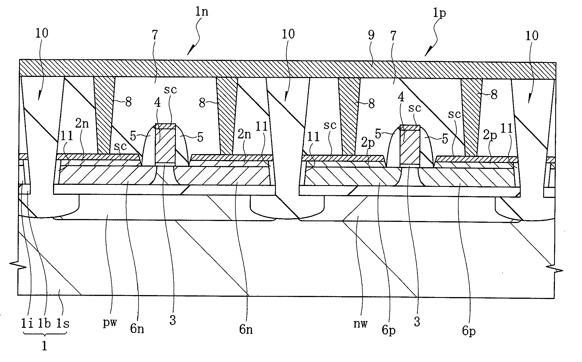
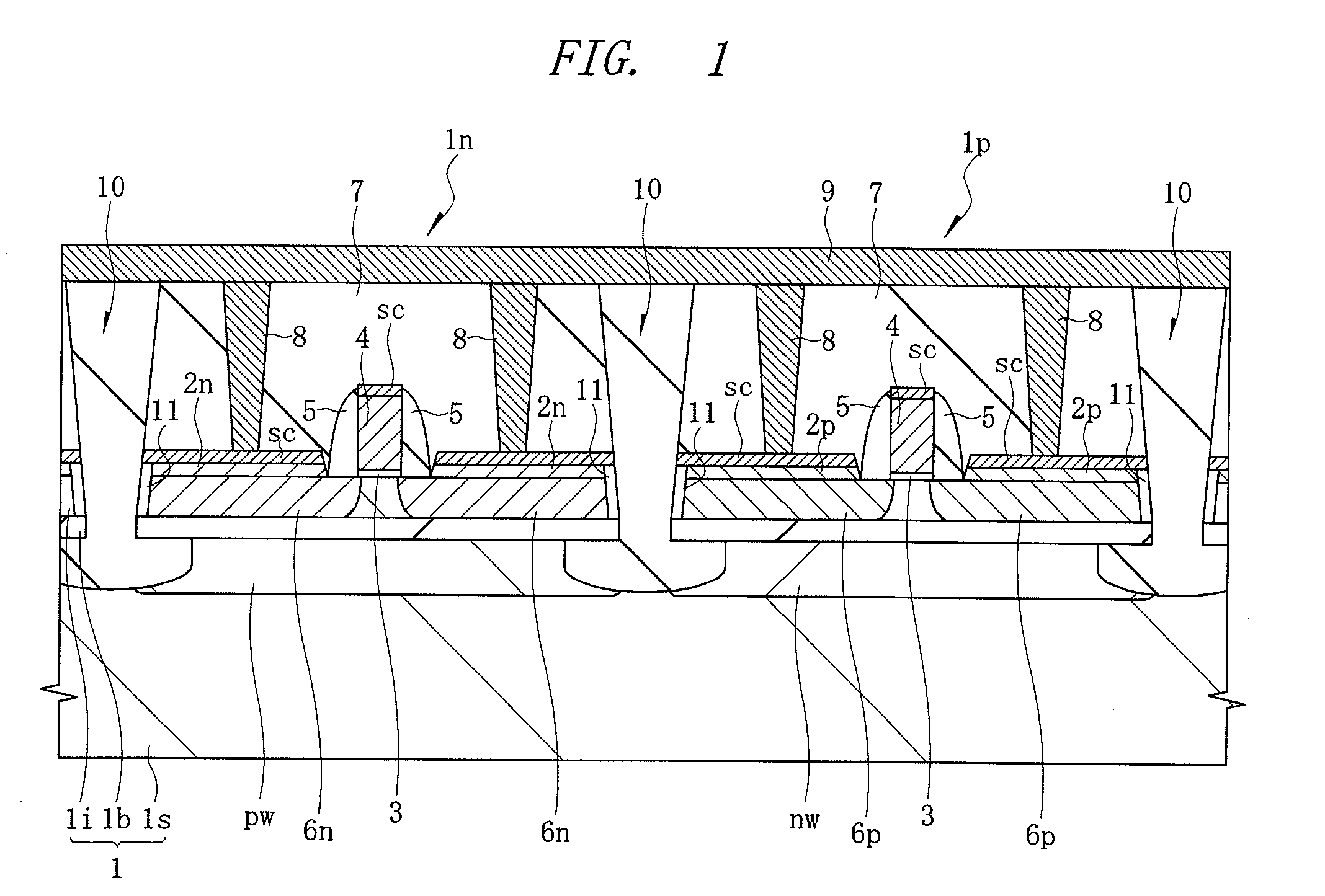
[0049]A semiconductor device and a manufacturing method thereof according to the first embodiment will be described in detail with reference to FIG. 1 to FIG. 15.

[0050]First, the structure of the semiconductor device according to the first embodiment will be described with reference to FIG. 1. FIG. 1 shows a cross-sectional view of the principal part of the semiconductor device according to the first embodiment.

[0051]The semiconductor device according to the first embodiment has an n channel MIS transistor 1n (hereinafter, simply referred to as nMIS n1) and a p channel MIS transistor 1p (hereinafter, simply referred to as pMIS p1) formed on a SOI substrate with a thin BOX layer 1. The SOI substrate with a thin BOX layer 1 is a substrate in which an SOI layer 1i is formed on a main surface of a silicon substrate 1s via a BOX layer 1b. A thickness of the BOX layer 1b is, for example, 3 nm to 50 nm and a typical thickness is, for example, 10 nm. Also, a thickness of the SOI layer 1i is...

second embodiment

[0108]A semiconductor device according to the second embodiment will be described while comparing with the above-described semiconductor device according to the first embodiment.

[0109]As shown in FIG. 16, the nMIS 1n and the pMIS 1p of the semiconductor device according to the second embodiment have a different structure in the principal part of the gate electrode 4 thereof from the above-described semiconductor device according to the first embodiment (see FIG. 1). Note that the semiconductor device according to the second embodiment has the similar structure to the semiconductor device according to the first embodiment other than the structure described below and also has the same effect, and the redundant description is omitted here.

[0110]In the nMIS 1n and the pMIS 1p of the semiconductor device according to the second embodiment, the gate insulating film 3 is formed along the inner side of the sidewalls 5, and a first gate electrode 12a and a second gate electrode 12b are embed...


PUM


Abstract

An n well and a p well disposed at a predetermined interval on a main surface of a SOI substrate with a thin BOX layer are formed, and an nMIS formed on the p well has a pair of n-type source/drain regions formed on semiconductor layers stacked on a main surface of the SOI layer at a predetermined distance, a gate insulating film, a gate electrode and sidewalls sandwiched between the pair of n-type source/drain regions. A device isolation is formed between the n well and the p well, and a side edge portion of the device isolation extends toward a gate electrode side more than a side edge portion of the n-type source/drain region (sidewall of the BOX layer).

Description

CROSS-REFERENCE TO RELATED APPLICATION[0001]The present application claims priority from Japanese Patent Application No. 2009-095755 filed on Apr. 10, 2009, the content of which is hereby incorporated by reference into this application.TECHNICAL FIELD OF THE INVENTION[0002]The present invention relates to a semiconductor device and a manufacturing technique thereof, and more particularly to a technique effectively applied to the manufacture of a device isolation provided in a substrate for electrically isolating a first semiconductor region of a first conductivity type and a second semiconductor region of a second conductivity type different from the first conductivity type.BACKGROUND OF THE INVENTION[0003]The speeding up, lower power consumption, multifunctionality and cost reduction have been demanded for a large-scale integrated circuit used in a microcomputer for a digital home appliance or a personal computer or an analog radio-frequency electronic component (for example, trans...

Claims


Application Information

Patent Timeline
IPC IPC(8): H01L27/12H01L21/336
CPCH01L21/76283H01L27/1203H01L21/84H01L21/823878
Inventor MORITA, YUSUKETSUCHIYA, RYUTAISHIGAKI, TAKASHIYOSHIMOTO, HIROYUKISUGII, NOBUYUKIKIMURA, SHINICHIRO
Owner HITACHI LTD
Why Eureka
Try Eureka