Semiconductor laser device and circuit for and method of driving same

a laser device and semiconductor technology, applied in the direction of laser optical resonator construction, laser details, laser output parameters control, etc., can solve the problems of increasing the cost of parallel ribbon fibers, increasing the difficulty of transmitting multiple wavelengths at the same time, and reducing the number of passive components. , the effect of eliminating costly and bulky bias tees

Active Publication Date: 2010-10-14
T&S COMM
View PDF9 Cites 23 Cited by
  • Summary
  • Abstract
  • Description
  • Claims
  • Application Information

AI Technical Summary

Benefits of technology

[0019]Some aspects of the invention provide a laser diode supplying sufficient optical power for multiple-wavelength optical transmission systems, with excellent wavelength control, while operating at a low enough electrical drive current for it to be driven by inexpensive low-power electronics.
[0021]One aspect of the invention provides a laser diode and associated bias and modulation circuit that can be connected to the laser diode driver with a significantly reduced number of passive components. In another aspect the invention provides a directly modulated laser in which the DC bias is applied to one section of the laser and the high-speed modulation signal is applied to a different section of the laser, which in some aspects eliminates costly and bulky bias tees. Some of the embodiments of the invention also achieve a reduction in electrical power dissipation by eliminating the AC coupling between the laser diode driver and the laser diode.

Problems solved by technology

However, the reach is limited as different modes of the fiber travel at different speeds and it is becomes more difficult to transmit multiple wavelength simultaneously.
The parallel ribbon fibers are of course quite expensive and connectors with 24 fibers inside are complicated to make, even if they use multimode fiber with looser alignment tolerance.
These lasers, however, have serious drawbacks in multiple wavelength links.
Also their small area and circular shape give them a high thermal resistance, and their output optical power is generally limited to below 1 milliwatt, especially at high temperature.
The optical elements that combine optical signals at different wavelengths into a single fiber inevitably introduce optical loss.
The disadvantage of conventional DFB lasers is they generally use a high electrical current drive relative to VCSELs.
Unfortunately it is difficult to achieve very low threshold current for a DFB laser, for example by reducing the length of the laser, because the required optical gain per unit length increases beyond what is easily achievable.
Another problem with shorter DFB lasers of for example 110 μm length is that it is difficult to cleave devices shorter than about 200 μm.
Regarding possible use of Distributed Bragg Reflector (DBR) laser designs, the disadvantages of this structure relate to the longitudinal optical mode control, since there is no grating in the active region.
A bigger problem is the tendency to “hop” from one wavelength to another as the drive current is changed.
This tendency means that there would be a narrow range of acceptable bias current for any individual laser, so device yield would be quite low and testing and calibration would be time consuming.
The electrical drive circuitry that supplies current to the laser diode is another cause of undesired power dissipation, because of its complexity and the general requirement to provide separate current paths for the direct current bias and the radio-frequency (RF) data signal.
This method only works well for relatively low bit rates (up to Mb / s) as the turn on delay of the laser and associated noise and laser response (laser relaxation oscillation) result in significant degradation of the transmitted signal for bit rates exceeding several Mb / s.
For optical links the RF content of the data covers a wide frequency spectrum resulting in an inductive path that typically consists of several low cost inductors and resistors, or costly high quality inductors.
This typical bias circuit, usually referred to as a bias tee, is not only large in size but also inefficient in terms of electrical power dissipation, as the DC component of the LDD output stage is not used in the LD due to the DC blocking of the coupling capacitors.
Variations on this, which add a laser driver final stage co-located in the laser package, use relatively large components inside the laser package, which is undesirable as well.

Method used


Image

  • Semiconductor laser device and circuit for and method of driving same
  • Semiconductor laser device and circuit for and method of driving same
  • Semiconductor laser device and circuit for and method of driving same

Examples


second embodiment

[0072]A second embodiment is to replace the 2-section DFB laser with a 2-section Fabry-Perot (FP) laser or distributed Bragg reflector (DBR) laser. In this embodiment the front facet or distributed reflector contributes to lasing of the rear section. Therefore the DC current to the rear section needs to be high enough such that the optical power emitted by the rear section is high enough to bleach through the front section as to provide enough reflected optical power from the front facet or front distributed reflector. In some embodiments the DBR laser may have a long waveguide including a short active region, for example with lengths of 600 microns and 100 microns, respectively.

third embodiment

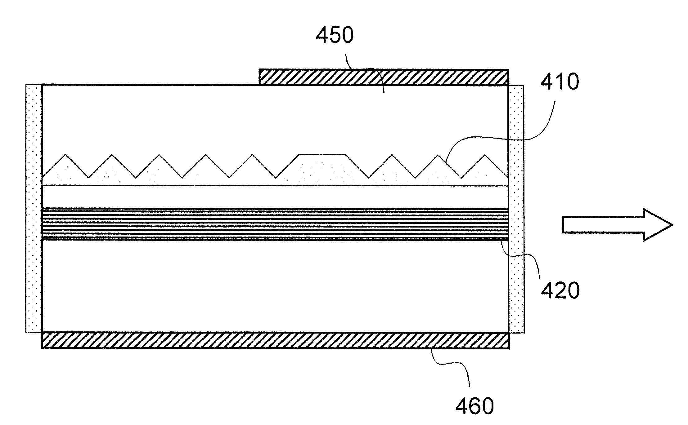
[0073]A third embodiment uses a three-section phase-shifted DFB laser with symmetric modulation, for example, as illustrated in FIG. 15. To maintain the single mode selectivity of the phase shifted DFB, the device has anti-reflection coatings on both facets, and is separated into three sections, two outer sections 1510 and 1520 and a middle section 1530. A current to the middle section is fixed above its lasing threshold. The two outer sections and facets are generally not essential in achieving lasing. The two outer sections are modulated in parallel from zero current to a modulation current that is split equally between the two outer sections. As the sections are electrically isolated and the modulated sections generally do not need a DC pre-bias current, there is no need for bias tees and the number of passive components in the circuit connecting the laser diode driver and the laser diode is significantly reduced.

[0074]A drawback of the third embodiment is that due to symmetry th...

ninth embodiment

[0079]A ninth embodiment is a variation on all previous embodiments using a laser driver that provides small adjustable DC pre-bias on the output lines without use of bias tees, allowing for some small pre-bias on the modulated section, which can improve the dynamic performance of the laser in certain cases.

[0080]Aspects of the invention therefore include directly modulated lasers in which modulation current is provided to only portions of the laser and methods and circuits for providing modulation current. Although the invention has been discussed with respect to various embodiments, it should be recognized that the invention includes the novel and non-obvious claims supported by this disclosure and the insubstantial variations of same.


PUM


Abstract

A directly driven laser includes multiple contacts, with at least one of the contacts for injecting current into the laser such that the laser reaches at least a lasing threshold and at least one of the contacts for providing a data signal to the laser. In some embodiments a differential data signal is effectively provided to a front and a rear section of the laser, while lasing threshold current is provided to a central portion of the laser.

Description

CROSS REFERENCE TO RELATED APPLICATIONS[0001]This application claims the benefit of the filing date of U.S. Provisional Application No. 61 / 163,748, filed Mar. 26, 2009, entitled “A Semiconductor Laser Device”, and U.S. Provisional Application No. 61 / 168,190, filed Apr. 9, 2009, entitled “A Method For Directly Modulating Lasers”; the disclosures of which are incorporated by reference.BACKGROUND OF THE INVENTION[0002]Optical fiber communications has generally replaced electrical links over long distances in the past few decades. In more recent past, optical links are being used at shorter distances to connect servers to switches and for datacenters.[0003]The advantages of fiber optics compared to electrical links are the greater bandwidth and reduced degradation of the signal with distance. At 10 Gb / s data rates, for the signal to travel more than 100-300 m in a fiber, generally single mode fiber is needed, with a typical mode size of about 8 microns. As an alternative, when distances...

Claims


Application Information

Patent Timeline
Patent Type & Authority Applications(United States)
IPC IPC(8): H01S5/06H01S5/30H01S5/12
CPCH01S5/028H01S5/0428H01S5/06226H01S5/125H01S5/12H01S5/124H01S5/06258
Inventor YOFFE, GIDEONPEZESHKI, BARDIASCHRANS, THOMAS P.
Owner T&S COMM
Why Eureka
Try Eureka