Photoelectric conversion device and manufacturing method thereof

a technology of conversion device and manufacturing method, which is applied in the manufacture of final products, basic electric elements, climate sustainability, etc., can solve the problems of difficult to form a single crystal silicon film having high photoelectric conversion efficiency, difficult to bend, twist, pressing force, etc., and achieve high mechanical strength and high efficiency. , the effect of saving resources

Inactive Publication Date: 2010-11-04
SEMICON ENERGY LAB CO LTD
View PDF27 Cites 29 Cited by
  • Summary
  • Abstract
  • Description
  • Claims
  • Application Information

AI Technical Summary

Benefits of technology

[0037]According to one embodiment of the present invention, a photoelectric conversion device can be provided in which a single crystal semiconductor is used for a photoelectric conversion layer and high efficiency and resource saving are attempted. When a light-transmitting insulating substrate is used as a supporting substrate and a semiconductor junction and an electrode are formed on the surface side of a semiconductor layer, a structure in which light enters on the substrate side, which has been difficult in a conventional structure, can be formed and a modular structure having high mechanical strength can be obtained. In addition, photoelectric conversion devices can be completed in a batch process for a plurality of single crystal semiconductor layers formed over a large-area substrate, and a method for manufacturing a photoelectric conversion device, the integration process of which is easy, can be provided.

Problems solved by technology

The substrate structure has characteristics of thin and light weight; on the other hand, there is a problem of low resistance to bending, twist, pressing force, or the like.
However, it is difficult to form a single crystal silicon film having high photoelectric conversion efficiency in a large area in a manner similar to that of a non-single-crystal silicon film, which is a significant challenge.

Method used


Image

  • Photoelectric conversion device and manufacturing method thereof
  • Photoelectric conversion device and manufacturing method thereof
  • Photoelectric conversion device and manufacturing method thereof

Examples


embodiment 1

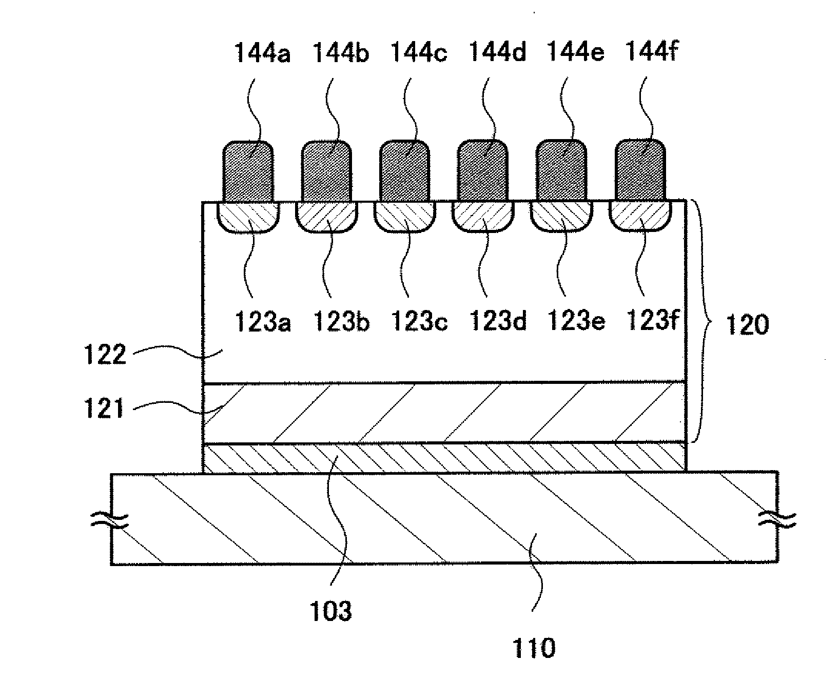
[0057]One embodiment of the present invention is a photoelectric conversion device having a single crystal semiconductor layer. A light-transmitting insulating substrate is used as a supporting substrate, semiconductor junctions and electrodes are formed on the surface side of the semiconductor layer, and a photo acceptance surface is provided on the supporting substrate side.

[0058]A cross-sectional view of a photoelectric conversion device provided with a photoelectric conversion layer over a base substrate is illustrated in FIG. 1. There are no particular limitations on the planar shape of the photoelectric conversion layer, and a rectangular shape including a square, a polygonal shape, or a circular shape can be employed.

[0059]There are no particular limitations on a base substrate 110 as long as the substrate can withstand a manufacturing process of a photoelectric conversion device according to one embodiment of the present invention and can have a light-transmitting property; ...

embodiment 2

[0075]One embodiment of the present invention is a photoelectric conversion device having a single crystal semiconductor layer. A light-transmitting insulating substrate is used as a supporting substrate, semiconductor junctions and an electrode are formed on the surface side of the semiconductor layer, and a photo acceptance surface is provided on the supporting substrate side.

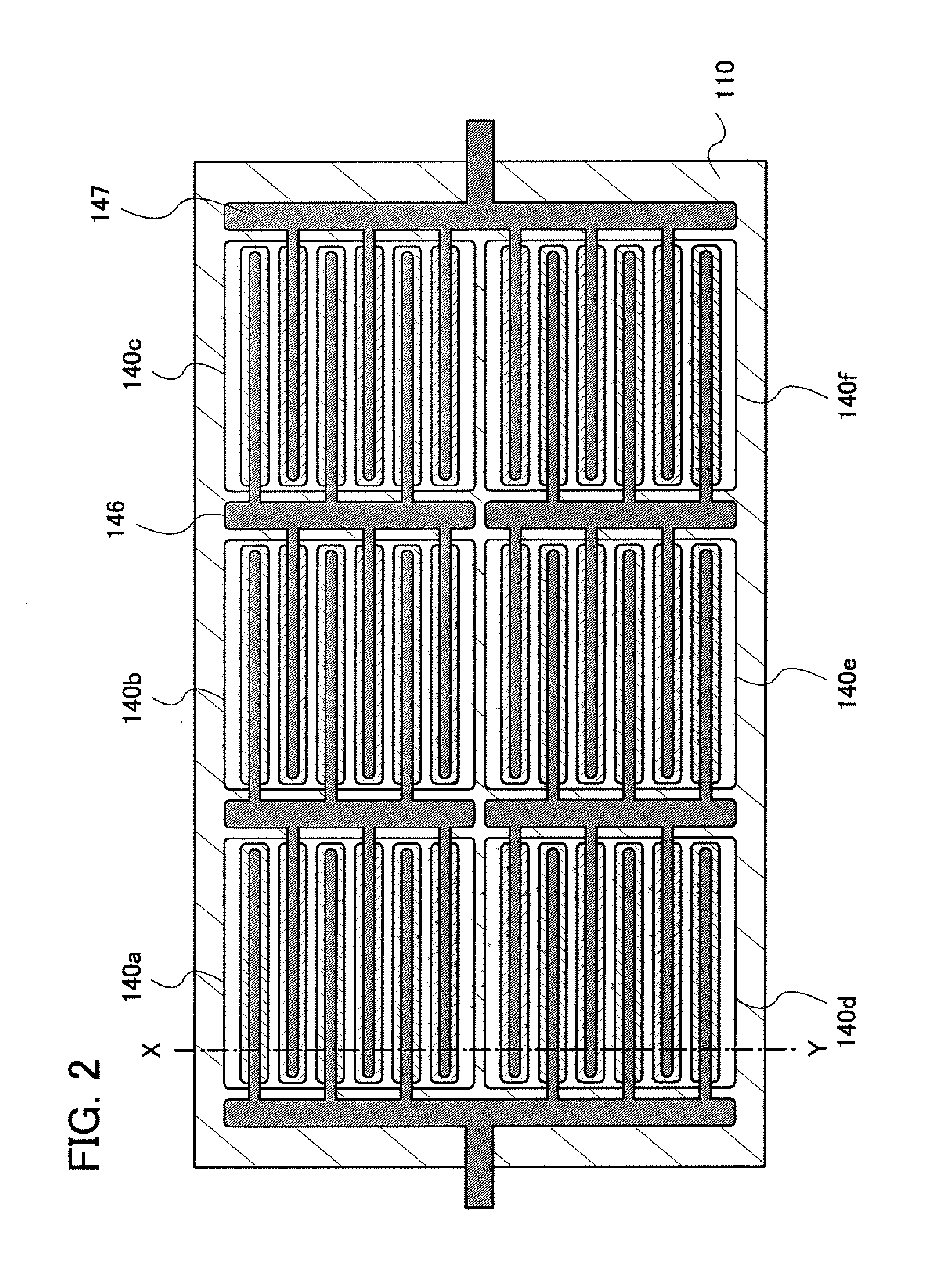
[0076]In this embodiment, a method for manufacturing a photoelectric conversion module will be described in details with reference to drawings.

[0077]Note that a photoelectric conversion module in this specification is a kind of photoelectric conversion device, and refers to a structure in which a plurality of photoelectric conversion layers is connected in series or in parallel in order to obtain desired power.

[0078]In FIG. 2, illustrated is an example in which a plurality of planar photoelectric conversion layers is arranged over one substrate having an insulating surface at predetermined intervals. Several ...

embodiment 3

[0178]In this embodiment, an example of a method for manufacturing a photoelectric conversion device, which is different from that described in Embodiment 2, will be described. Note that the description of a portion which overlaps with the above embodiments is omitted or partially simplified.

[0179]As illustrated in FIG. 5B, stack bodies formed using the insulating layer 103, the first single crystal semiconductor layer 121, and the second single crystal semiconductor layer 122 are formed over the base substrate 110 in accordance with Embodiment 2.

[0180]Over the stack bodies, first impurity semiconductor layers 230a, 230c, and 230e and second impurity semiconductor layers 230b, 230d, and 230f are alternately formed in a band shape with no overlap. Over the impurity semiconductor layers, first electrodes 240a, 240c, and 240e and second electrodes 240b, 240d, and 240f are formed, so that the photoelectric conversion device can be completed (see FIGS. 14A, 14B, and 14C and FIG. 16A).

[01...


PUM


Abstract

To provide a novel photoelectric conversion device and a manufacturing method thereof. Over a base substrate having a light-transmitting property, a light-transmitting insulating layer and a single crystal semiconductor layer over the insulating layer are formed. A plurality of first impurity semiconductor layers each having one conductivity type is provided in a band shape in a surface layer of the single crystal semiconductor layer or on a surface of the single crystal semiconductor layer, and a plurality of second impurity semiconductor layers each having a conductivity type which is opposite to the one conductivity type is provided in a band shape in such a manner that the first impurity semiconductor layers and the second impurity semiconductor layers are alternately provided and do not overlap with each other. First electrodes in contact with the first impurity semiconductor layers and second electrodes in contact with the second impurity semiconductor layers are provided, and a back contact cell is formed, whereby a photoelectric conversion device provided with a photo acceptance surface on the base substrate side is formed.

Description

BACKGROUND OF THE INVENTION[0001]1. Field of the Invention[0002]The present invention relates to a photoelectric conversion device and a manufacturing method thereof.[0003]2. Description of the Related Art[0004]Global warming has advanced, and energy sources which replace fossil fuels have been reviewed. Of them, a photoelectric conversion device which is also called a solar battery holds the greatest promise as a typical electric power generating means in the next generation. In recent years, research and development of the device has been actively carried out, and a market has rapidly expanded.[0005]The photoelectric conversion devices are attractive power generation means which use inexhaustible sunlight as energy sources and which do not emit carbon dioxide at the time of power generation. However, there are problems in that photoelectric conversion efficiency per unit area is not sufficient, that the amount of power generation is affected by the daylight hours under present con...

Claims


Application Information

Patent Timeline
Patent Type & Authority Applications(United States)
IPC IPC(8): H01L31/00H01L21/78H01L31/18
CPCY02E10/547H01L31/075H01L31/022425H01L31/1896H01L31/028H01L31/068H01L31/1864H01L31/03682H01L31/1892H01L31/0682Y02E10/546Y02E10/548Y02P70/50
Inventor SHIMOMURA, AKIHISAISAKA, FUMITOKATO, SHO
Owner SEMICON ENERGY LAB CO LTD
Why Eureka
Try Eureka