Production of semiconductor devices

Active Publication Date: 2010-11-04
QUANTUM NIL LTD +1
View PDF13 Cites 66 Cited by
  • Summary
  • Abstract
  • Description
  • Claims
  • Application Information

AI Technical Summary

Benefits of technology

[0068]The hydride-vapor phase epitaxy (HVPE), also called chloride transport chemical vapor deposition, of GaN is a relatively well-established process based on the gaseous transport of the group III and group V elements to the deposition zone of a growth reactor. In this technique, Cl is used to transport the group-III species instead of organometallic sources in the MOCVD technique. This has a distinct advantage in that large growth rates (up to 200 μm/hr) can be achieved by this technique over the MOCVD or the MBE methods (≦2 μm/hr). In contrast to MOCVD, which is a non-equilibrium cold-wall reactor-based technique, HVPE is a reversible equilibrium-based process in which a hot-wall reactor is employed. The typical growth procedure is as follows. Sapphire, silicon carbide, zinc oxides or other compatible substrates are inserted into the deposition zone of the growth chamber and heated. When the final growth temperature is reached the NH3 flow is started. After a period to allow the NH3 concentration to reach a steady-state value, HCl flow is started to provide transport of the gallium chloride (GaCl), which is synthesized by reacting HCl gas with liquid Ga metal in the Ga zone at 800-900° C. via the reaction: 2HCl(g)+2Ga(l)→2GaCl(g)+H2(g). An alternative method of synthesis is by reacting Chlorine gas with Ga metal around 125° C. Then gaseous GaCl is transported from the Ga zone to the deposition zone to react with NH3 at 900-1200° C. to form GaN via the reaction GaCl(g)+NH3(g)→GaN(s)+HCl(g)+H2(g). Another major advantage of the HVPE growth method is the mutual annihilation of mixed dislocations lowering the defect densities in thicker GaN.
[0069]The use of fabricated GaN nano-columns, for example, as the compliant layer to grow GaN has several advantages. The mechanical confinement occurs between the interface of the nano-columns and top lateral grown layer due to the small diameter and the high aspect ratio of the column (height versus diameter). The stress and dislocations are mostly localized in the interface between the GaN nano-columns and the top lateral grown layer. Thus growth leads to the top lateral overgrowth layer being nearly free of stress and dislocations. In addition, the defects caused by the mosaic structure in conventional GaN films, arising from a spread of initial island misorientations can be minimized, since badly misoriented nano-columns eventually grow out, improving the general alignment. The topography of nano-columns with a narrow air gap permits coalescence with a very thin overgrown layer. Typically only ˜0.1-0.2 μm thickness is required for continuous overgrown GaN layers. This narrow air gap will also facilitate the very fast coalescence to form continuous AlN by the epitaxial lateral overgrowth of Al

Problems solved by technology

Despite the technological advances of the last few years, one of the key obstacles preventing further developments in GaN devices is the lack of high quality and commercially available low-cost, free-standing GaN templates.
These factors can significantly affect the performance and lifeti

Method used


Image

  • Production of semiconductor devices
  • Production of semiconductor devices
  • Production of semiconductor devices

Examples


example 1

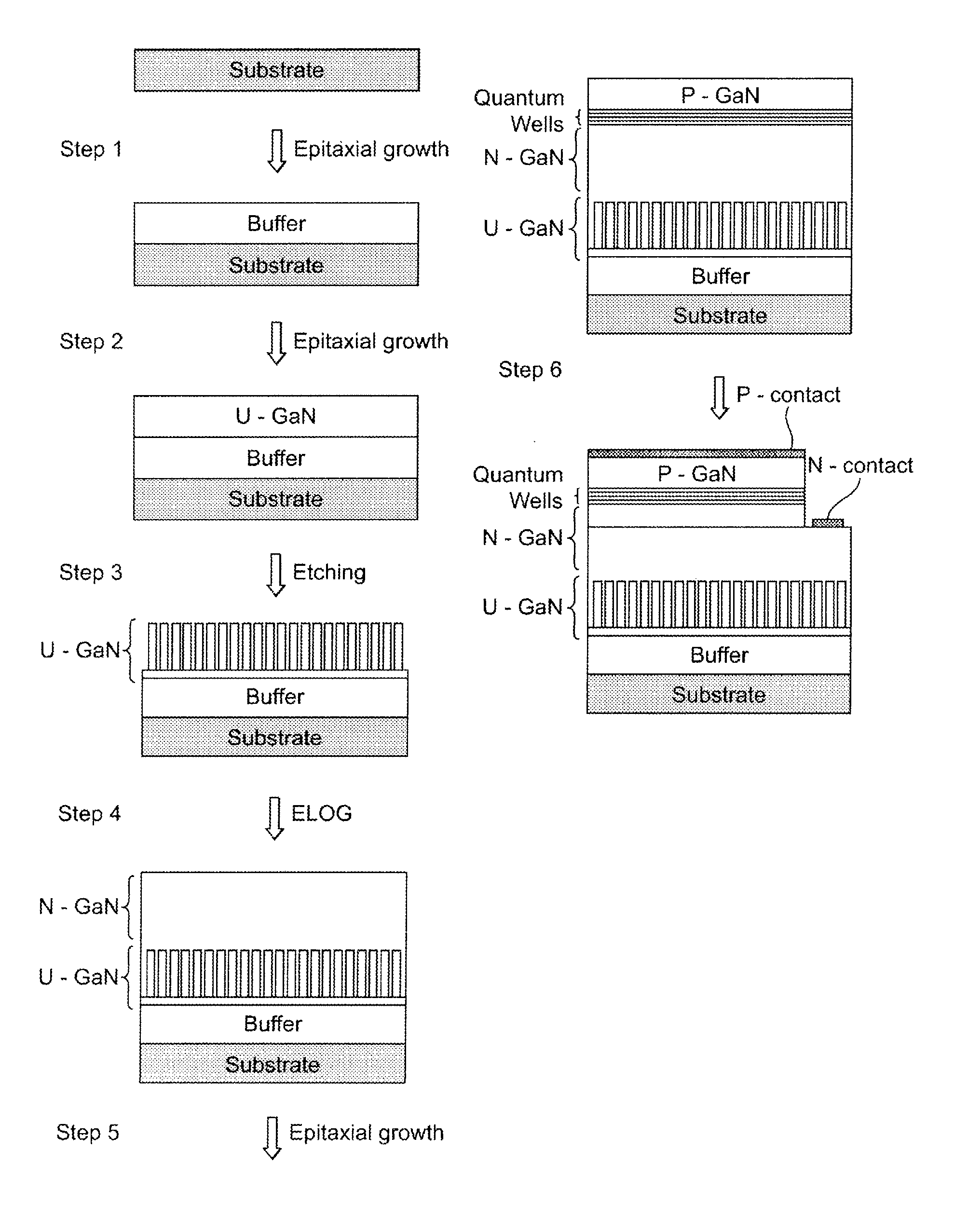
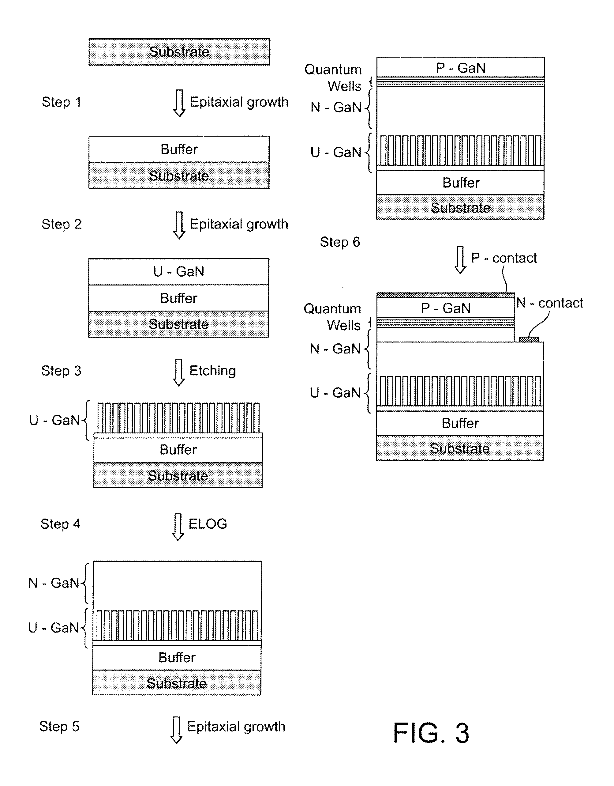
[0079]Example 1 relates to the growth and fabrication of full light emitting diode (LED) devices with insulating substrates. FIG. 3 schematically shows the process flow for such a method. Each device is attached to the nano-column substrate. The nano-column substrate enhances the light extraction from the top. The low strain and low defect lateral-grown layer improves the internal quantum efficiency of the devices.

[0080]In this Example, a c-plane-oriented sapphire substrate of about 2 inches (5.08 cm) in diameter is used, on which a buffer of GaN grown at around 350-550° C. of about 20 nm thickness, followed by undoped GaN of about 1 μm thickness is epitaxially grown as shown in Step 1 of FIG. 3. Un-doped U—GaN of about 2-3 μm is deposited by MOCVD (Step 2 of FIG. 1) to form the template for the fabrication of nano-columns. Before loading, the GaN template is degreased in KOH for few seconds, rinsed in de-ionized water, etched in a H2SO4 / H3PO4=3:1 solution at about 80° C. for few mi...

example 2

[0088]Similarly to Example 1, the initial epitaxial lateral overgrowth is carried out by a MOCVD growth process. However, in this Example, trimethylaluminum (TMA) partially or totally replaces the trimethylgallium (TMG) used in Example 1 to grow an AlGaN layer.

[0089]Epitaxial growth of the full device, in this case an LED, is continued in the MOCVD reactor. The LED structure grown comprises the following layers: an n-type Si-doped AlGaN layer (about 1.5-2 μm), an AlxGa1−xN / AlyGa1−yN MQW active region (about 35 Å / 100 Å, 2-6 pairs, and y≧x+0.03), an AlGaN:Mg capping layer (˜200 Å), and p-type Mg-doped AlGaN (about 0.2-0.3 μm). The electron and hole concentration in the AlGaN:Si and AlGaN:Mg layers are about 1018 cm−3 and 6×1017 cm−3 respectively. The LEDs produced are suitable for producing light of UV region wavelength.

example 3

[0090]In this Example, the template used is a-plane GaN or AlGaN grown on top of a γ-plane sapphire substrate. Otherwise the production of nano-columns is as described for Examples 1 or 2. This template has particular advantage that it may be used to grow a non-polar semiconductor layer, which may be especially beneficial for the fabrication of optical components such as white LEDs (see below).

[0091]Epitaxial growth of the full device, in this case an LED, is continued in the MOCVD reactor. The LED structure produced comprises the following layers: an n-type Si-doped GaN layer (about 1.5-2 μm), an InGaN / GaN MQW active region (6 pairs QWs, with the quantum well width of 25, 35, 45, 55, 75, 90 Å and barrier of 100 Å), an AlGaN:Mg capping layer (˜200 Å), and p-type Mg-doped GaN (about 0.2-0.3 μm). The electron and hole concentration in the GaN:Si and GaN:Mg layers are about 3×1018 cm−3 and 6×1017 cm−3, respectively. This device will give a much broader bandwidth than conventional LEDs,...


PUM


Abstract

A method of producing a layered semiconductor device comprises the steps of: (a) providing a base comprising a plurality of semiconductor nano-structures, (b) growing a semiconductor material onto the nano-structures using an epitaxial 5 growth process, and (c) growing a layer of the semiconductor material using an epitaxial growth process.

Description

CROSS-REFERENCE TO RELATED APPLICATION[0001]The present application is the National Stage of International Application No. PCT / GB2008 / 050063, filed Jan. 31, 2008, which claims the benefit under 35 U.S.C. §119 of United Kingdom Application No. 0702560.4, filed Feb. 9, 2007 and United Kingdom Application No. 0708281.1, filed Apr. 30, 2007, both of which are incorporated herein by reference in their entirety.FIELD OF THE INVENTION[0002]The present invention relates to a method of producing a layered semiconductor device and a semiconductor device thus produced.BACKGROUND[0003]Wide band-gap GaN and related materials are recognized to be among the most attractive compound semiconductors for use in a variety of devices. They are adapted for optoelectronic and microelectronic devices which operate in a wide spectral range, from visible to ultraviolet and in the high temperature / high power applications area. The main advantages of nitride semiconductors in comparison with other wide-band-ga...

Claims


Application Information

Patent Timeline
IPC IPC(8): H01L29/06H01L21/20
CPCH01L21/0237H01L21/02433H01L21/02439H01L21/0265H01L21/0254H01L21/02639H01L21/02645H01L21/02513C30B25/18H01L21/20B82B3/00B82Y40/00
Inventor WANG, WANG NANG
Owner QUANTUM NIL LTD
Why Eureka
Try Eureka