Method for creating s/tem sample and sample structure

a technology of transmission electron microscope and sample structure, which is applied in the field of preparation of samples and analysis methods for scanning transmission electron microscope and transmission electron microscope, can solve the problems of destroying much consuming time, and affecting the quality of the original sample, so as to increase the throughput and reproducibility of tem analysis, and the process of creating and analysing tem samples is less labor-intensive.

Active Publication Date: 2010-12-02
FEI CO
View PDF11 Cites 53 Cited by
  • Summary
  • Abstract
  • Description
  • Claims
  • Application Information

AI Technical Summary

Benefits of technology

[0020]An object of the invention, therefore, is to provide an improved method for TEM sample analysis. Preferred embodiments of the present invention provide improved methods for TEM sample creation, especially for small geometry (<100 nm thick) TEM lamella...

Problems solved by technology

As features continue to get smaller and smaller, however, there comes a point where the features to be measured are too small for the resolution provided by an ordinary SEM.
Because a sample must be very thin for viewing with transmission electron microscopy (whether TEM or STEM), preparation of the sample can be delicate, time-consuming work.
The disadvantage to these techniques is that they are not site-specific and often require that the starting material be sectioned into smaller and smaller pieces, thereby destroying much of the original sample.
The smaller back trench is primarily to save time, but the smaller trench also prevents the finished sample from falling over flat into larger milled trenches which may make it difficult to remove the specimen during the micromanipulation operation...

Method used


Image

  • Method for creating s/tem sample and sample structure
  • Method for creating s/tem sample and sample structure
  • Method for creating s/tem sample and sample structure

Examples


Embodiment Construction

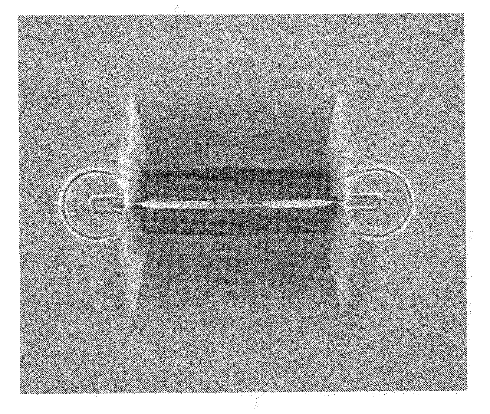
[0041]Preferred embodiments of the present invention provide improved methods for lamella creation. A preferred embodiment can create S / TEM samples with a thickness in the 50-100 nm range for the purposes of S / TEM metrology with minimal site-to-site variation. The process can produce a 10 μm wideט5 μm deepט500 nm thick lamella with a final-thinned window of 3 μm×3 μm at the targeted final thickness (50-100 nm). S / TEM samples produced according to the present invention will not suffer from bowing phenomenon when thinned to 100 nm or less and are robust enough to survive automated extraction and mounting.

[0042]A preferred method or apparatus of the present invention has many novel aspects, and because the invention can be embodied in different methods or apparatuses for different purposes, not every aspect need be present in every embodiment. Moreover, many of the aspects of the described embodiments may be separately patentable.

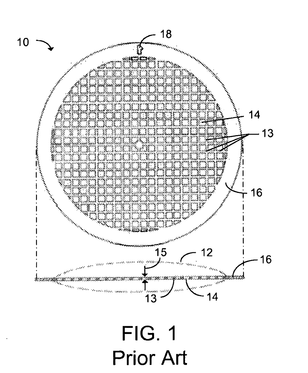
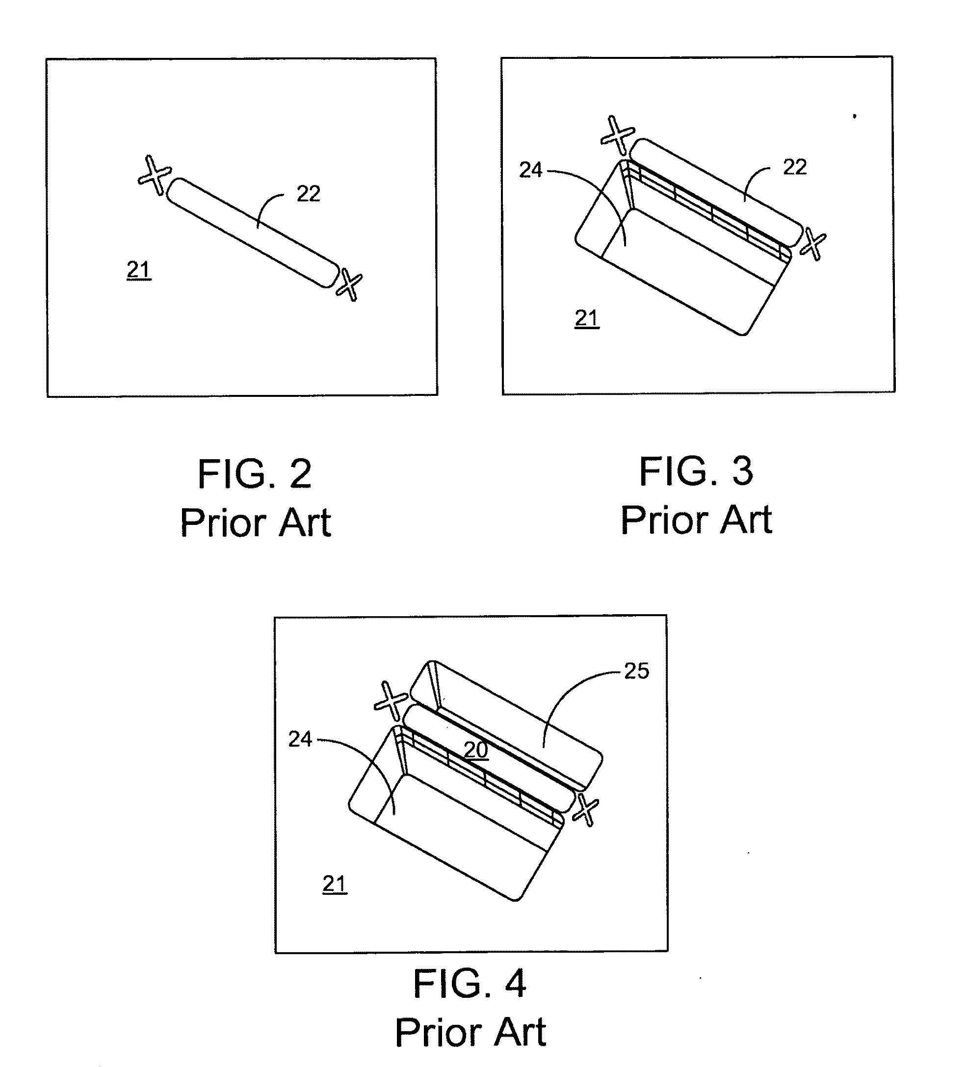
[0043]Current TEM lamella creation processes for...


PUM

PropertyMeasurementUnit
Timeaaaaaaaaaa
Thicknessaaaaaaaaaa
Thicknessaaaaaaaaaa

Abstract

An improved method and apparatus for S/TEM sample preparation and analysis. Preferred embodiments of the present invention provide improved methods for TEM sample creation, especially for small geometry (<100 nm thick) TEM lamellae. A novel sample structure and a novel use of a milling pattern allow the creation of S/TEM samples as thin as 50 nm without significant bowing or warping. Preferred embodiments of the present invention provide methods to partially or fully automate TEM sample creation, to make the process of creating and analyzing TEM samples less labor intensive, and to increase throughput and reproducibility of TEM analysis.

Description

[0001]The present application claims priority from PCT Application No. PCT / US2007 / 082159, filed Oct. 22, 2007, and from U.S. Prov. Pat. App. No. 60 / 853,183, filed Oct. 20, 2006, which are hereby incorporated by reference.TECHNICAL FIELD OF THE INVENTION[0002]The present invention relates to preparation of samples and methods of analysis for transmission electron microscopes and scanning transmission electron microscopes.BACKGROUND OF THE INVENTION[0003]Semiconductor manufacturing, such as the fabrication of integrated circuits, typically entails the use of photolithography. A semiconductor substrate on which circuits are being formed, usually a silicon wafer, is coated with a material, such as a photoresist, that changes solubility when exposed to radiation. A lithography tool, such as a mask or reticle, positioned between the radiation source and the semiconductor substrate casts a shadow to control which areas of the substrate are exposed to the radiation. After the exposure, the ...

Claims


Application Information

Patent Timeline
IPC IPC(8): G01N1/32G01N1/04
CPCG01N1/32H01J37/3056H01J2237/208H01J2237/31745G01N23/04H01J37/26G01N1/06G01N1/08G01N1/28H01J37/20H01J37/06H01J37/18H01J37/28H01J2237/063H01J2237/182H01J2237/204H01J2237/2802H01J2237/31749
Inventor BLACKWOOD, JEFFSTONE, STACEY
Owner FEI CO
Why Eureka
Try Eureka