
Photovoltaic Power Generation System and Photovoltaic Power Generation Device

a photovoltaic power generation and photovoltaic technology, applied in the direction of electric variable regulation, process and machine control, instruments, etc., can solve the problems of reducing the operating current by an amount corresponding and the cell may suffer from a loss of power, so as to reduce the number of components, and reduce the effect of quantum efficiency

Inactive Publication Date: 2010-12-02
SMART SOLAR INT
View PDF9 Cites 11 Cited by
  • Summary
  • Abstract
  • Description
  • Claims
  • Application Information

AI Technical Summary

Benefits of technology

[0006]In order to substantially improve conversion efficiency, a method is used in which multiple semiconductors, each having a different band gap, are stacked on top of each other. This method uses semiconductors having high quantum efficiency in different wavelength bands and therefore prevents light energy from being consumed as heat energy. The use of a wide band-gap semiconductor naturally provides a high operating voltage, but operating current decreases by an amount corresponding to unused light energy. However, each semiconductor can obtain an operating current corresponding to its own p-n junction by maintaining the operating current constant, which improves conversion efficiency. Such a solar cell, which is generally referred to as a tandem cell or a triple cell, is an effective solution to extract wide-range light energy efficiently and can be expected to work effectively in any types of solar batteries.

Problems solved by technology

The use of a wide band-gap semiconductor naturally provides a high operating voltage, but operating current decreases by an amount corresponding to unused light energy.
As a method for improving efficiency, semiconductors each made of the same kinds of materials or different kinds of materials are stacked so as to utilize the band gaps of the semiconductors to ensure sensitivity suitable for the energy spectrum of sunlight; however, it is required to design the cells to maintain the current flow constant, otherwise the cells may suffer from a loss of power.

Method used


Image

  • Photovoltaic Power Generation System and Photovoltaic Power Generation Device
  • Photovoltaic Power Generation System and Photovoltaic Power Generation Device
  • Photovoltaic Power Generation System and Photovoltaic Power Generation Device

Examples


embodiment 1

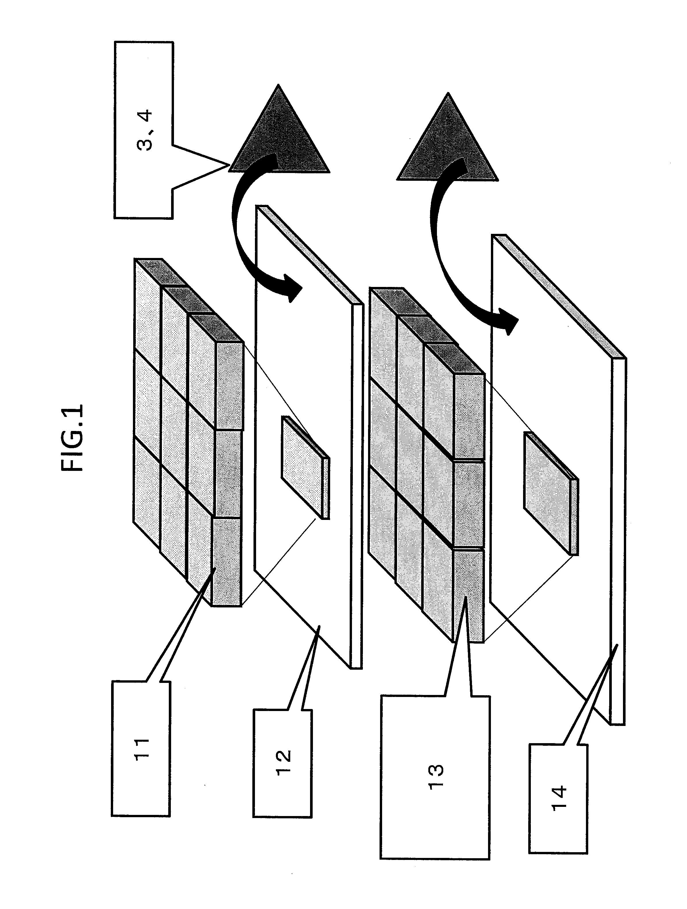
[0065]FIG. 1 illustrates a basic concept of the photovoltaic power generation system according to Embodiment 1 of the present invention. Silicon and germanium, both crystallize in the diamond structure with a lattice constant of 0.543 nm and 0.565 nm, respectively, and that is to say, the silicon and germanium are lattice-mismatched semiconductor materials. Substrates employed for both the silicon and germanium are a single-crystalline direction p-type substrate. The surface layer is doped to be an n-type diffused layer. A silver electrode is formed on a part of the front surface as an n-type electrode, while an aluminum electrode is formed on a part of the back surface as a p-type electrode. A germanium cell 13 is divided into 121 sections (11×11), each of which being connected in series with a transparent insulating substrate 14. Similarly, a silicon cell 11 is divided into 49 sections (7×7), each of which being connected in series with a transparent insulating quartz substrate 1...

embodiment 2

[0078]Silicon and gallium-aluminum arsenide (GaAlAs) have a lattice constant of 0.543 nm and 0.562 to 0.563 nm, respectively, which belong to a group in which an epitaxial growth technique cannot be used because it causes distortion. Table 3 shows the characteristics of cells per unit area and data of modules per 100 cm2.

[0079]As a lower first cell, a silicon cell was used. An upper second cell was made of GaAlAs. The GaAlAs cell and silicon cell were mounted on a transparent insulating substrate such as a quartz, respectively, and stacked. The output of each cell was extracted at a load resistor and a step-up voltage transformer (booster). When light is irradiated at an air mass (AM) of 1.5 and current is maintained constant at 0.027 A, the output voltages of the output circuits are 17.4 V and 16.6 V, respectively. The voltages are combined in series, resulting in 40 V in total. The solar batteries are designed to change the output voltage with changes in illumination.

[0080]It is g...

embodiment 3

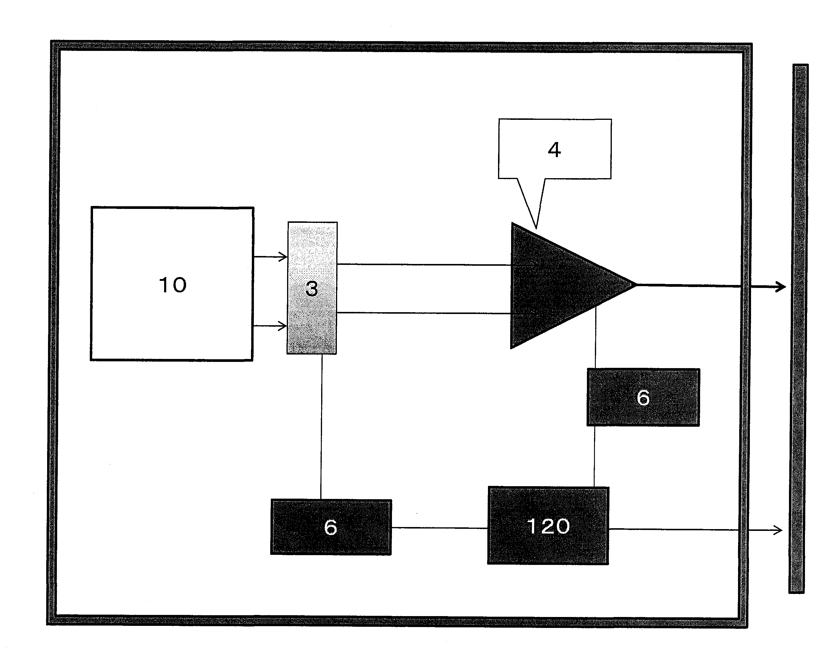
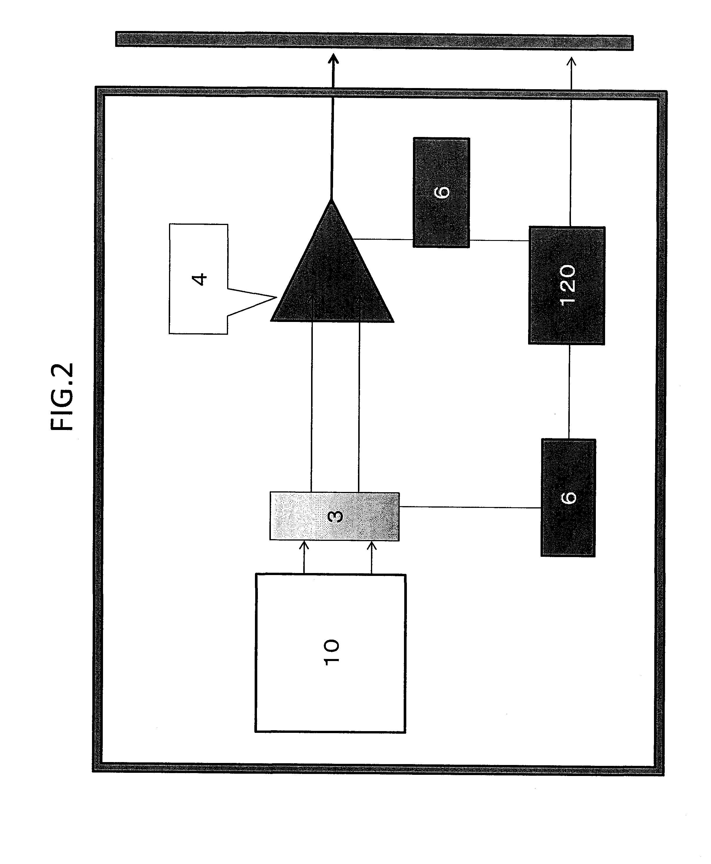
[0081]When stacked solar cell modules are manufactured, a terminal box in which a connection terminal unit is installed is attached to every module. The wiring diagram of the connection terminal unit is shown in FIG. 7. An input from the solar cell module is introduced through terminals 1 and terminals 2. The terminals 1 have a higher potential than that of the terminals 2. The terminals 1 and 2 are connected to load resistors 3 and the inputs are fed to step-up voltage transformers (boosters) 4. Outputs from the step-up voltage transformers (boosters) 4 are introduced from back-flow prevention diodes 5 to connecting terminals 8 and 10 where the outputs are combined. The combined output power is extracted from output terminals 100 and 110. A communication IC chip 120 is connected to communication lines. Although there are two inputs in FIG. 7, it is needless to say that the number of the inputs can be increased to three, four or more. FIG. 8 shows a structure of a voltage-controllab...


PUM


Abstract

It is an object to obtain a photovoltaic power generation system. A photovoltaic power generation system includes multiple solar cell modules each having a different band gap and step-up voltage transformers (boosters) that receive outputs from load resistors, the load resistors being controlled to maximize outputs of the respective solar cell modules. An output voltage of each step-up voltage transformer (booster) is controlled to be a predetermined output voltage (or output current), and the step-up voltage transformers (boosters) are connected in parallel (or in series) to obtain predetermined electric power.

Description

BACKGROUND OF THE INVENTION[0001](1) Field of the Invention[0002]The present invention relates to a photovoltaic power generation system and a photovoltaic power generation device.[0003](2) Description of the Related Art[0004]Solar battery cells fall into two broad categories: one made of two kinds of semiconductors that form a p-n junction; and the other, which is called a dye-sensitized type cell, using dyes dispersed in ceramics. The solar battery of the present invention features both categories. It is known that the open-circuit voltage of a cell used in a solar battery is in general approximately 0.4 V lower than mainly the band gap width of the cell. In addition, the maximum electric power of the cell can be obtained by controlling the load impedance; however, the operating voltage is generally even lower than the open-circuit voltage. Thus, a solar battery requires multiple cells connected with each other in series. The multiple series-connected cells are generally referred ...

Claims


Application Information

Patent Timeline
Patent Type & Authority Applications(United States)
IPC IPC(8): H02J4/00H01L31/042H01L31/05H01L31/052H02S40/34
CPCH01L31/02021H02M7/493Y02E10/52Y02E10/542H01L2924/0002Y02E10/56H01L2924/00Y02E10/548H01L31/043G05F1/67H02J7/35
Inventor TOMITA, TAKASHI
Owner SMART SOLAR INT
Learn More