Semiconductor memory device, manufacturing method thereof, data processing system, and data processing device

a memory device and semiconductor technology, applied in the direction of diodes, digital storage, instruments, etc., can solve the problems of reduced current of a selection element, small occupied area per one selection element, and complex manufacturing process of mos transistor in a three-dimensional structure, so as to reduce leakage current, reduce the degree of integration, and reduce the formation pitch of pn-j unction diodes

Inactive Publication Date: 2010-12-02
ELPIDA MEMORY INC
View PDF6 Cites 3 Cited by
  • Summary
  • Abstract
  • Description
  • Claims
  • Application Information

AI Technical Summary

Benefits of technology

[0015]As explained above, according to the present invention, the pillar-shaped pn-j unction diodes and the memory elements are formed in a self-aligned manner. Therefore, a formation pitch of the pn-j unction diodes can be made small. As a result, the degree of integration can be increased more than a conventional level. Further, because the pillar-shaped pn-junction diodes are constituted by a part of the semiconductor substrate, various problems attributable to the use of the selective epitaxial method do not occur. As a result, it is possible to provide a semiconductor memory device having less leakage current, less variation in manufacturing, and a high degree of integration.

Problems solved by technology

However, when the degree of integration of a device becomes higher, an occupied area per one selection element becomes small.
Therefore, there is a problem that an ON current of a selection element is reduced.
However, a manufacturing process of a MOS transistor in a three-dimensional structure is very complex, and a substantial increase in the ON current cannot be expected.
Therefore, the use of diodes as selection elements is not suitable for a voltage-sensing semiconductor memory device such as a DRAM, and is suitable for a current-sensing semiconductor memory device.
Therefore, a misalignment unavoidably occurs in positions on a plane.
This becomes a hindrance in increasing the degree of integration.
Therefore, many crystal defects occur in silicon pillars, and these defects become a cause of increasing a leakage current.
A silicon growth by the selective epitaxial method does not necessarily proceed uniformly on the plane, and has a large variation in manufacturing.
Further, when the degree of integration becomes very high, the speed of silicon growth by the selective epitaxial method becomes slow, and the growth does not proceed in some cases.
The above problems occur in not only PRAMs but also in other semiconductor memory devices using pillar-shaped pn-junction diodes as selection elements.
Further, because the pillar-shaped pn-junction diodes are constituted by a part of the semiconductor substrate, various problems attributable to the use of the selective epitaxial method do not occur.

Method used


Image

  • Semiconductor memory device, manufacturing method thereof, data processing system, and data processing device
  • Semiconductor memory device, manufacturing method thereof, data processing system, and data processing device
  • Semiconductor memory device, manufacturing method thereof, data processing system, and data processing device

Examples


Embodiment Construction

[0016]The above features and advantages of the present invention will be more apparent from the following description of certain preferred embodiments taken in conjunction with the accompanying drawings, in which:

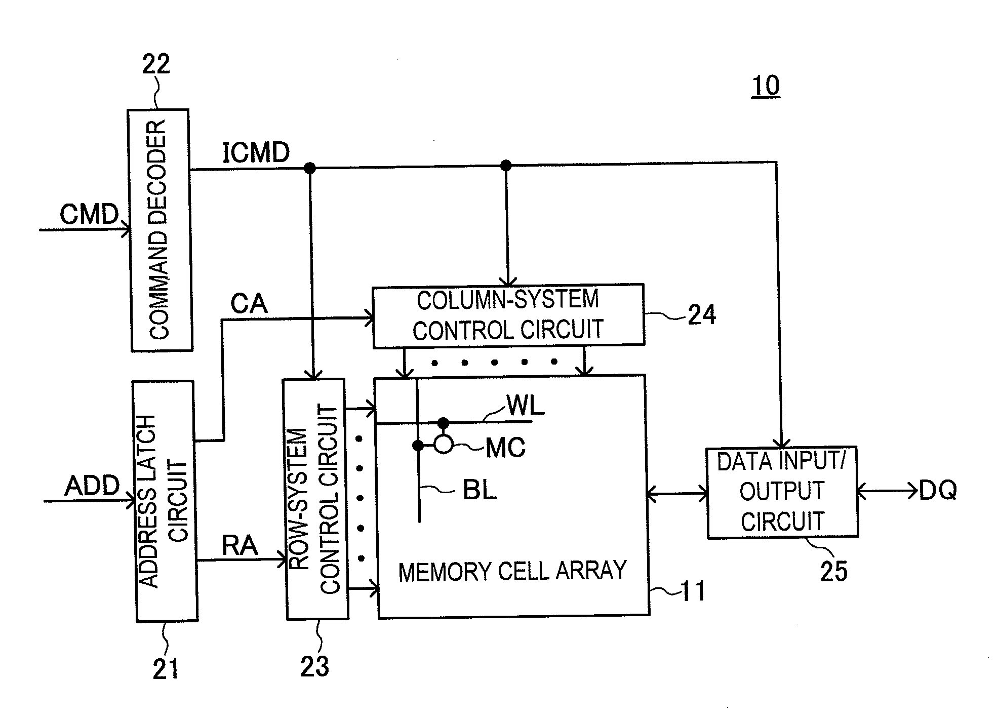
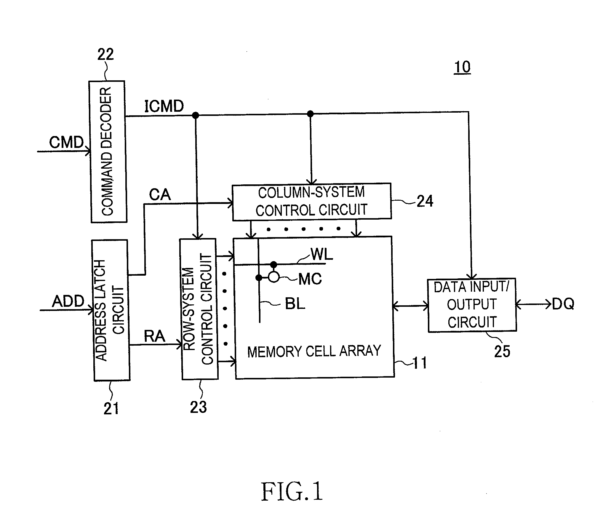
[0017]FIG. 1 is a block diagram of a semiconductor memory device 10 according to an embodiment of the present invention;

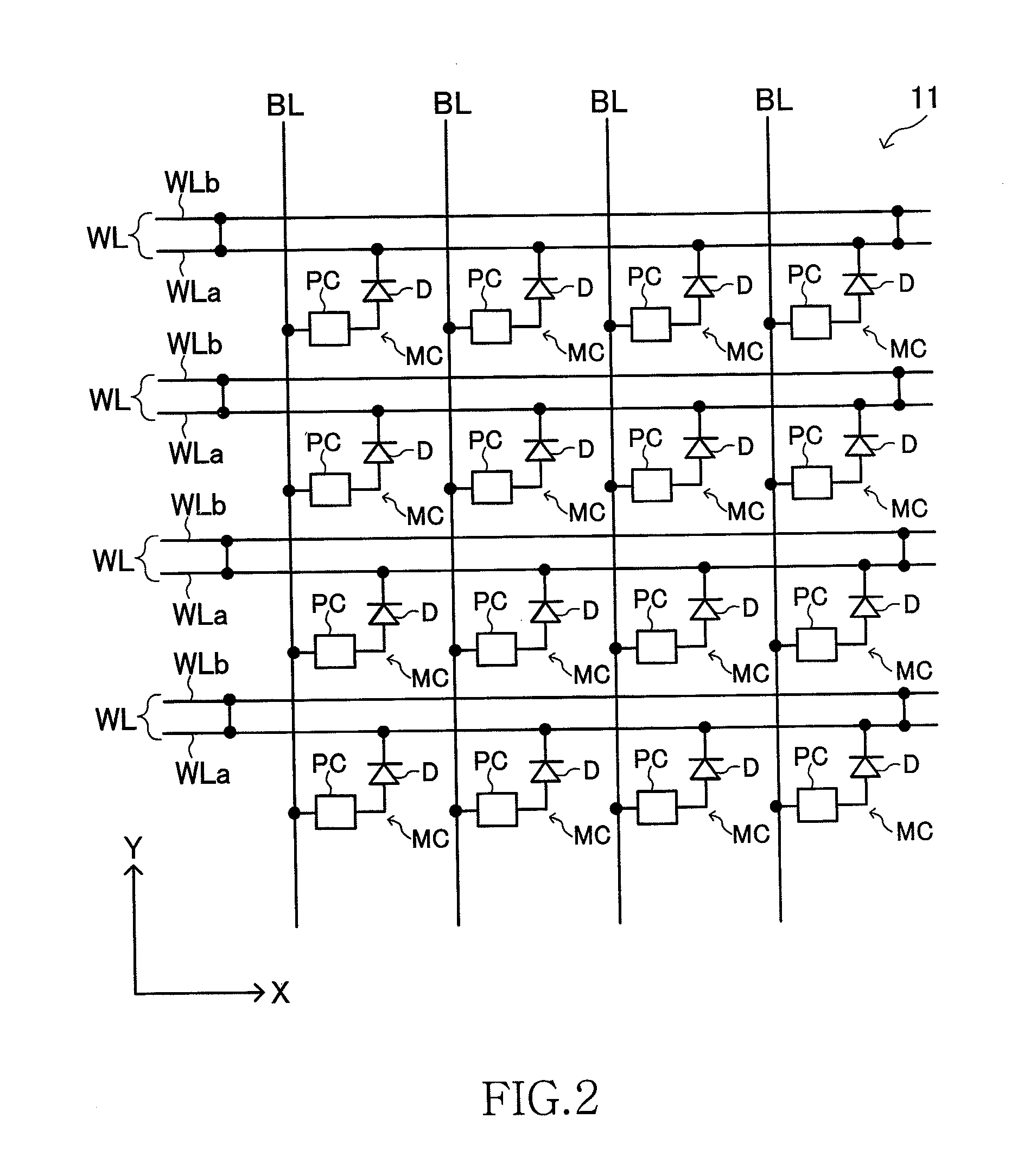
[0018]FIG. 2 is a circuit diagram showing a part of the memory cell array 11 in detail;

[0019]FIGS. 3A and 3B show a device configuration of the memory cell MC, where FIG. 3A shows a cross-sectional view, and FIG. 3B shows a plan view;

[0020]FIGS. 4A and 4B show a view showing a process (formation of a hard mask 105) in the manufacturing processes of the semiconductor memory device 10, where FIG. 4A shows a cross-sectional view, and FIG. 4B shows a plan view;

[0021]FIGS. 5A and 5B show a view showing a process (etching of p-type impurity diffusion layer 104) in the manufacturing processes of the semiconductor memory device 10, where FIG. 5A shows a cross-sect...


PUM


Abstract

A semiconductor memory device includes: first and second impurity diffusion layers that form a part of a semiconductor substrate, each of the impurity diffusion layers function as one and the other of an anode and a cathode, respectively of a pn-junction diode; a recording layer connected to the second impurity diffusion layer; and a cylindrical sidewall insulation film provided on the first impurity diffusion layer. At least a part of the second diffusion layer and at least a part of the recording layer are formed in a region surrounded by a sidewall insulation film. According to the present invention, because a pillar-shaped pn-junction diode and the recording layer are formed in a self-aligned manner, the degree of integration of a semiconductor memory device can be increased. Further, because a silicon pillar is a part of the semiconductor substrate, a leakage current attributable to a crystal defect can be reduced.

Description

BACKGROUND OF THE INVENTION[0001]1. Field of the Invention[0002]The present invention relates to a semiconductor memory device and a manufacturing method thereof, and more particularly relates to a semiconductor memory device using pn-j unction diodes as a selection element and a manufacturing method of the semiconductor memory device. The present invention also relates to a data processing system and a data processing device, which include memory cells using pn-junction diodes.[0003]2. Description of Related Art[0004]Most of semiconductor memory devices in practical application at present are configured such that a number of memory elements are arranged in a matrix in an X direction and a Y direction. To access a specific one of these memory elements, any one of plural selection lines (word lines) arranged in the X direction is activated to make it possible to access the memory element via a signal line (a bit line) arranged in the Y direction. More specifically, memory elements an...

Claims


Application Information

Patent Timeline
Patent Type & Authority Applications(United States)
IPC IPC(8): G11C11/00H01L45/00H01L21/04
CPCG11C13/0004G11C2213/72H01L27/1021H01L27/115H01L27/11517H01L27/2409H01L27/2463H01L45/06H01L45/1233H01L45/143H01L45/144H01L45/148H10B63/20H10B63/80H10N70/231H10N70/8825H10N70/884H10N70/8828H10N70/826H10B41/00H10B69/00
Inventor KAWAGOE, TSUYOSHIASANO, ISAMU
Owner ELPIDA MEMORY INC
Why Eureka
Try Eureka