Establishing a hydrophobic surface of sensitive low-k dielectrics of microstructure devices by in situ plasma treatment

a low-k dielectric, hydrophobic technology, applied in the field of microstructures, can solve the problems of not being able to readily etch copper on the basis of well-established plasma assisted etch recipes, the patterning of continuous copper layers with a thickness that is appropriate for forming metal lines may not be compatible with presently available etch strategies, and the severity of severe problems residing in copper's, etc., to achieve enhanced deposition processes, reduce the degree of surface damage, and enhance the surface characteristics of silicon oxid

Inactive Publication Date: 2010-12-02
ALSEPHINA INNOVATIONS INC
View PDF5 Cites 17 Cited by
  • Summary
  • Abstract
  • Description
  • Claims
  • Application Information

AI Technical Summary

Benefits of technology

[0014]Generally, the present disclosure relates to techniques for enhancing the surface characteristics of silicon oxide based low-k dielectric materials by re-establishing a hydrophobic surface structure which may be “damaged” by plasma assisted processes, such as plasma etching, resist stripping, plasma enhanced deposition processes and the like. In this respect, a hydrophobic surface is to be understood such that the amount of methyl groups is higher than an amount of polarizable functional groups, such as OH groups. The amount of functional groups and the type thereof may be efficiently determined by Fourier transformed infrared spectroscopy (FTIR). For this purpose, a plasma treatment may be performed in situ on the basis of an appropriate precursor gas, thereby initiating a reaction with dangling surface bonds of the “damaged” surface area in order to maintain or re-establish the desired hydrophobic nature of the exposed surface. Due to the in situ nature, i.e., the “repair” plasma ambient may be established in the same plasma-confining process environment as the “damaging” plasma ambient, a very efficient mechanism in terms of repair efficiency and overall manufacturing efficiency may be accomplished since the desired hydrophobic functional groups may be immediately bonded to the damaged surface area without requiring additional process reactors, transport activities and the like. Moreover, since the “repair” plasma ambient may be readily established in a plurality of conventional plasma reactors, such as plasma etch tools, plasma assisted deposition tools and the like, the mechanism of establishing or re-establishing the hydrophobic functional groups at the surface area may be performed at any appropriate stage of a plasma-based manufacturing process, such as an etch process, so that generally a significantly reduced degree of surface damage may be created, which may even be substantially completely re-established at a final phase or immediately after the prece

Problems solved by technology

The introduction of copper into the fabrication of microstructures and integrated circuits comes along with a plurality of severe problems residing in copper's characteristics to readily diffuse in silicon dioxide and other dielectric materials, as well as the fact that copper may not be readily patterned on the basis of well-established plasma assisted etch recipes.
For example, based on conventional plasma assisted etch processes, copper may not substantially form any volatile etch byproducts such that the patterning of a continuous copper layer with a thickness that is appropriate for forming metal lines may not be compatible with presently available etch strategies.
Although silicon nitride and related materials may have excellent diffusion blocking capabilities, using silicon nitride as an interlayer dielectric material is less than desirable due to the moderately high dielectric constant, which may result in a non-acceptable performance degradation of the metallization system.
Although the permittivity of these dielectric materials may be reduced by incorporating carbon and forming a corresponding porous structure, which may result in a very increased surface area at interface regions connecting to other materials, the overall mechanical and chemical characteristics of these low-k and ultra low-k (ULK) materials may also be significantly altered and may

Method used


Image

  • Establishing a hydrophobic surface of sensitive low-k dielectrics of microstructure devices by in situ plasma treatment
  • Establishing a hydrophobic surface of sensitive low-k dielectrics of microstructure devices by in situ plasma treatment
  • Establishing a hydrophobic surface of sensitive low-k dielectrics of microstructure devices by in situ plasma treatment

Examples


Embodiment Construction

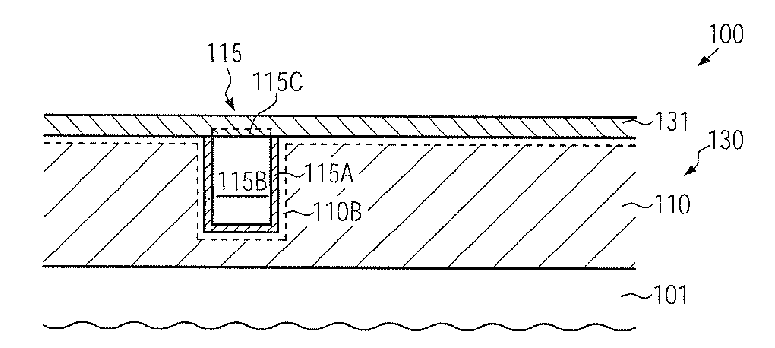
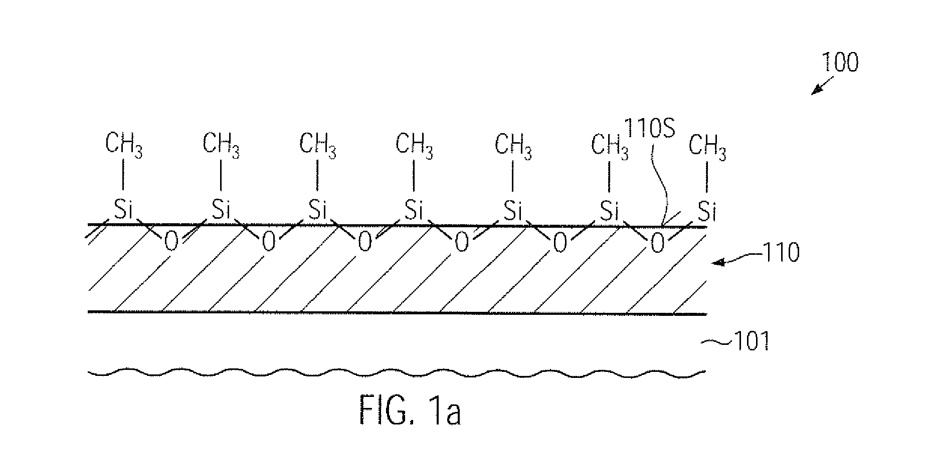
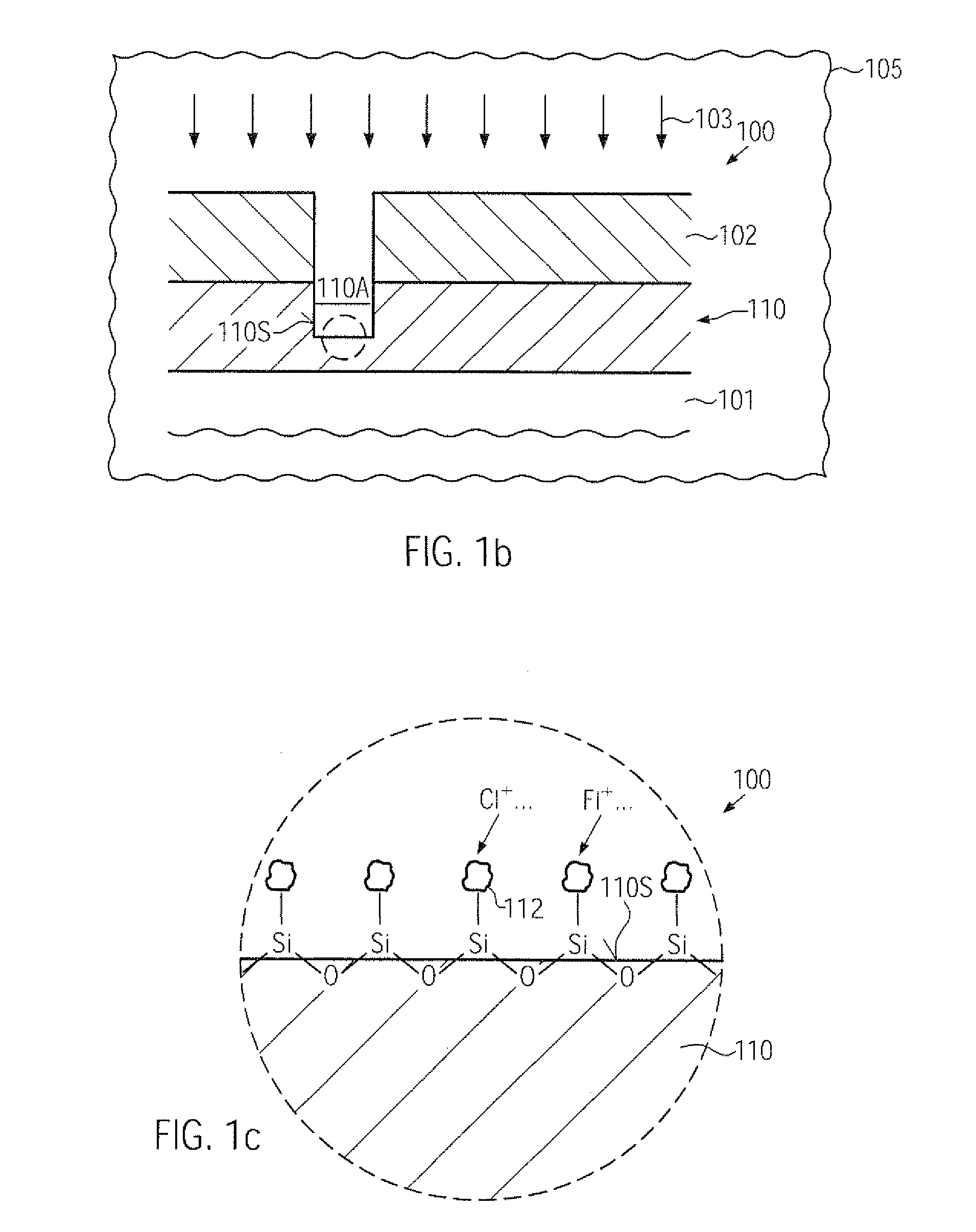
[0029]Various illustrative embodiments of the invention are described below. In the interest of clarity, not all features of an actual implementation are described in this specification. It will of course be appreciated that in the development of any such actual embodiment, numerous implementation-specific decisions must be made to achieve the developers' specific goals, such as compliance with system-related and business-related constraints, which will vary from one implementation to another. Moreover, it will be appreciated that such a development effort might be complex and time-consuming, but would nevertheless be a routine undertaking for those of ordinary skill in the art having the benefit of this disclosure.

[0030]The present subject matter will now be described with reference to the attached figures. Various structures, systems and devices are schematically depicted in the drawings for purposes of explanation only and so as to not obscure the present disclosure with details ...


PUM


Abstract

Silicon oxide based low-k dielectric materials may receive superior hydrophobic surface characteristics on the basis of a plasma treatment using hydrogen and carbon containing radicals. For this purpose, the surface of the low-k dielectric material may be exposed to these radicals, at least in one in situ process in combination with another reactive plasma ambient, for instance used for patterning the low-k dielectric material. Consequently, superior surface characteristics may be established or re-established without significantly contributing to product cycle time.

Description

BACKGROUND OF THE INVENTION[0001]1. Field of the Invention[0002]Generally, the present disclosure relates to microstructures, such as advanced integrated circuits, and, more particularly, to material systems including silicon oxide based dielectrics having a low dielectric constant.[0003]2. Description of the Related Art[0004]In the fabrication of modern microstructures, such as integrated circuits, there is a continuous drive to improve performance in view of operational behavior and diversity of functions integrated in a single microstructure device. For this purpose, there is an ongoing demand to steadily reduce the feature sizes of microstructure elements, thereby enhancing the functionality of these structures. For instance, in modern integrated circuits, minimum feature sizes, such as the channel length of field effect transistors, have reached the deep sub-micron range, thereby increasing performance of these circuits in terms of speed and / or power consumption and / or diversit...

Claims


Application Information

Patent Timeline
IPC IPC(8): H01L21/768H01L21/31
CPCH01L21/3105H01L21/76814H01L21/76826H01L21/76829
Inventor FISCHER, DANIELSCHALLER, MATTHIAS
Owner ALSEPHINA INNOVATIONS INC
Why Eureka
Try Eureka