Two-Transistor Floating-Body Dynamic Memory Cell

a dynamic memory cell and floating-body technology, applied in digital storage, instruments, semiconductor devices, etc., can solve the problems of affecting the scalability and performance affecting the scalability of the memory cell, so as to improve the scalability and performance

Inactive Publication Date: 2010-12-30
UNIV OF FLORIDA RES FOUNDATION INC
View PDF12 Cites 29 Cited by
  • Summary
  • Abstract
  • Description
  • Claims
  • Application Information

AI Technical Summary

Benefits of technology

[0005]Embodiments of the present invention relate to memory. Embodiments of the present invention provide a DRAM that can be embedded in CMOS integrated logic circuits. Embodiments of a two-transistor memory cell are provided that can yield an improved scalability and performance compared to current one transistor memory cells. According to the present invention, one of the two transistors functions as a composite floating body / gate.
[0006]According to embodiments of the present invention a memory is provided utilizing a two-transistor memory cell where the body of the first transistor is coupled to the gate of the second transistor. A word line and two bit lines are used for manipulation of the two transistors. In one embodiment, the sources of the first and second transistor are coupled to ground, the drain of the first transistor is coupled to the first bit line, and the drain of the second transistor is coupled to the second bit line. In another embodiment, utilizing gate-induced drain leakage (GIDL) current (the floating body / gate cell (FBGC)), the source and drain of the first transistor are coupled to the first bit line, the drain of the second transistor is coupled to the second bit line, and the source of the second transistor is coupled to ground. In yet another embodiment, a modified FBGC is provided where the source region of the first transistor is implanted at high concentration with impurities of the same conductive type as the body of the first transistor. The source region having such implanted impurities can facilitate the coupling of the body of the first transistor structure to the gate of the second transistor. The first bit line can be coupled to only the drain of the first transistor structure.

Problems solved by technology

A conventional dynamic random access memory (DRAM) cell uses a stack capacitor or a deep-trench capacitor for storage, which is leading to prohibitive processing complexity as the memory technology is scaled [1].
While FinFET CMOS technology could enable scaling of the 1T FBC to gate lengths (Lg) less than 10 nm [12], there are other issues that tend to inhibit mainstream adaptation of the 1T FBC utilizing FinFET technology.
In particular, the 1T FBC utilizing FinFET technology relies on current sensing of the stored data, which can be less desirable than conventional voltage sensing because of more sophisticated sense amplifiers and added power consumption.
The 1T FBC utilizing FinFET technology requires the noted bias-induced accumulation, which can complicate the cell / chip design, undermine reliability, and sacrifice layout area.
In addition, because the attainable ΔVt is fundamentally limited, several paralleled fins are needed to increase the device effective width and current to get acceptable ΔIDS, thus severely under mining the memory density actually achievable.

Method used


Image

  • Two-Transistor Floating-Body Dynamic Memory Cell
  • Two-Transistor Floating-Body Dynamic Memory Cell
  • Two-Transistor Floating-Body Dynamic Memory Cell

Examples


Embodiment Construction

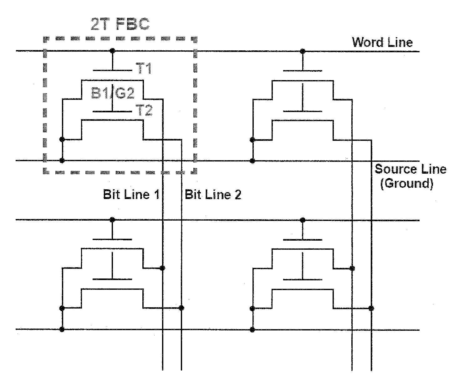
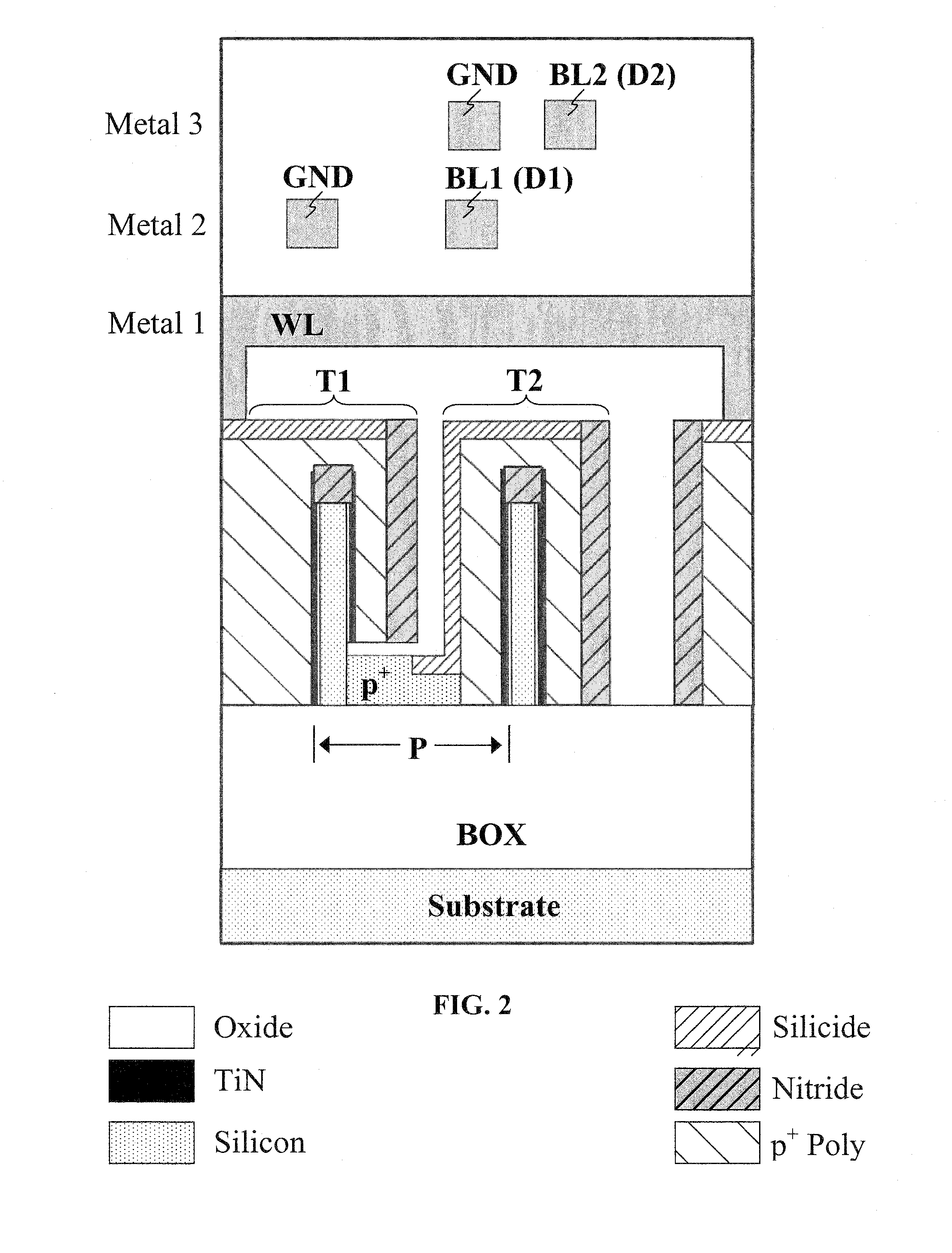
[0030]Embodiments of the present invention relate to memory. Embodiments of the subject technology provide a two-transistor floating-body cell for DRAM applications. An embodiment can involve a memory cell including a first transistor (T1) and a second transistor (T2), where the body (B1) of T1 is connected to the gate (G2) of T2. In operation, write / erase operations involve charging / discharging T1 and read operations involve reading T2. Three signal lines can be used: a word line, a first bit line, and a second bit line. In an embodiment, one bit line connects all drain nodes of the T1 transistors in a column of a DRAM array for programming the cells, and the second bit line connects all drain nodes of the T2 transistors in the column for sensing the data. The gate of T1 is tied to the word line.

[0031]In one embodiment, the source of T1 and the source of T2 are tied to ground. This embodiment can be referred to as a two-transistor floating body cell (2T-FBC). In another embodiment,...


PUM


Abstract

Embodiments relate to a two-transistor (2T) floating-body cell (FBC) for embedded-DRAM applications. Further embodiments pertain to a floating-body / gate cell (FBGC), which yields reduction in power dissipation, in addition to better signal margin, longer data retention, and higher memory density.

Description

CROSS-REFERENCE TO RELATED APPLICATIONS[0001]The present application is the U.S. National Stage Application of International Patent Application No. PCT / US2008 / 078460, filed on Oct. 1, 2008, which claims the benefit of U.S. Provisional Application Ser. No. 60 / 976,691, filed Oct. 1, 2007, and claims the benefit of U.S. Provisional Application Ser. No. 61 / 017,941, filed Dec. 31, 2007, all of which are hereby incorporated by reference herein in their entirety, including any figures, tables, or drawings.BACKGROUND OF INVENTION[0002]A conventional dynamic random access memory (DRAM) cell uses a stack capacitor or a deep-trench capacitor for storage, which is leading to prohibitive processing complexity as the memory technology is scaled [1]. Accordingly, study and development of “capacitorless” one-transistor (1T) DRAM cells that utilize the floating body of a silicon-on-insulator (SOI) metal oxide semiconductor field effect transistor (MOSFET) as the storage element have intensified [2]-...

Claims


Application Information

Patent Timeline
Patent Type & Authority Applications(United States)
IPC IPC(8): G11C7/00H01L27/12
CPCG11C11/404G11C2211/4016H01L27/108H01L29/785H01L27/10826H01L29/7841H01L27/10802H10B12/20H10B12/36H10B12/00
Inventor FOSSUM, JERRY G.MATHEW, LEOSADD, MICHAELTRIVEDI, VISHAL P.
Owner UNIV OF FLORIDA RES FOUNDATION INC
Why Eureka
Try Eureka