Semiconductor field effect transistor and method for fabricating the same

a semiconductor and field effect technology, applied in the direction of semiconductor devices, basic electric elements, electrical appliances, etc., can solve the problems of limiting the amplification of high frequency signals or fast switching, and it is almost impossible to improve the drain current density by applying a forward gate bias, and achieves large forward gate bias, high performance, and high mobility

Inactive Publication Date: 2011-01-20
SUMITOMO CHEM CO LTD +1
View PDF13 Cites 83 Cited by
  • Summary
  • Abstract
  • Description
  • Claims
  • Application Information

AI Technical Summary

Benefits of technology

[0023]According to the present invention, since a channel layer is formed at a similar semiconductor crystal layer interface with small electron scattering, high mobility can be provided. Furthermore, since optimal dielectric constant is disposed on the surface of the crystal layer, a large forward gate bias can be also applied. As a result, a high performance field effect transistor that achieves extremely large drain current density can be provided, which has an extreme significance in industrial uses.

Problems solved by technology

However, there are problems that since electrons run on an interface of different crystal system, the electron transit speed becomes insufficient by scattering due to crystal lattice disorder at the interface, and therefore there is a limit on amplification of high frequency signal or fast switching.
However, in the case of the GaN-HEMT, it is almost impossible to improve the drain current density by applying a forward gate bias.

Method used


Image

  • Semiconductor field effect transistor and method for fabricating the same
  • Semiconductor field effect transistor and method for fabricating the same
  • Semiconductor field effect transistor and method for fabricating the same

Examples


example 1

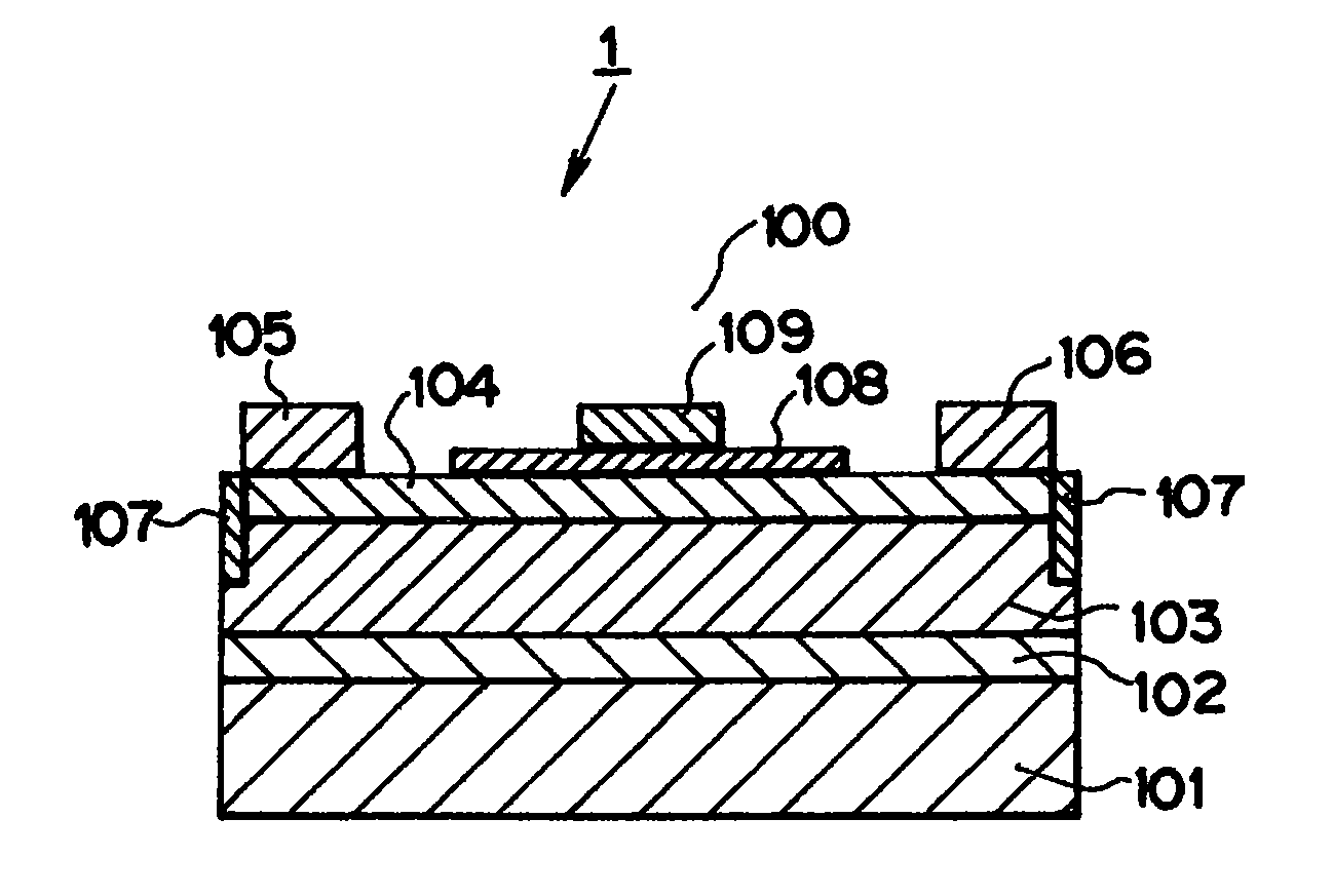
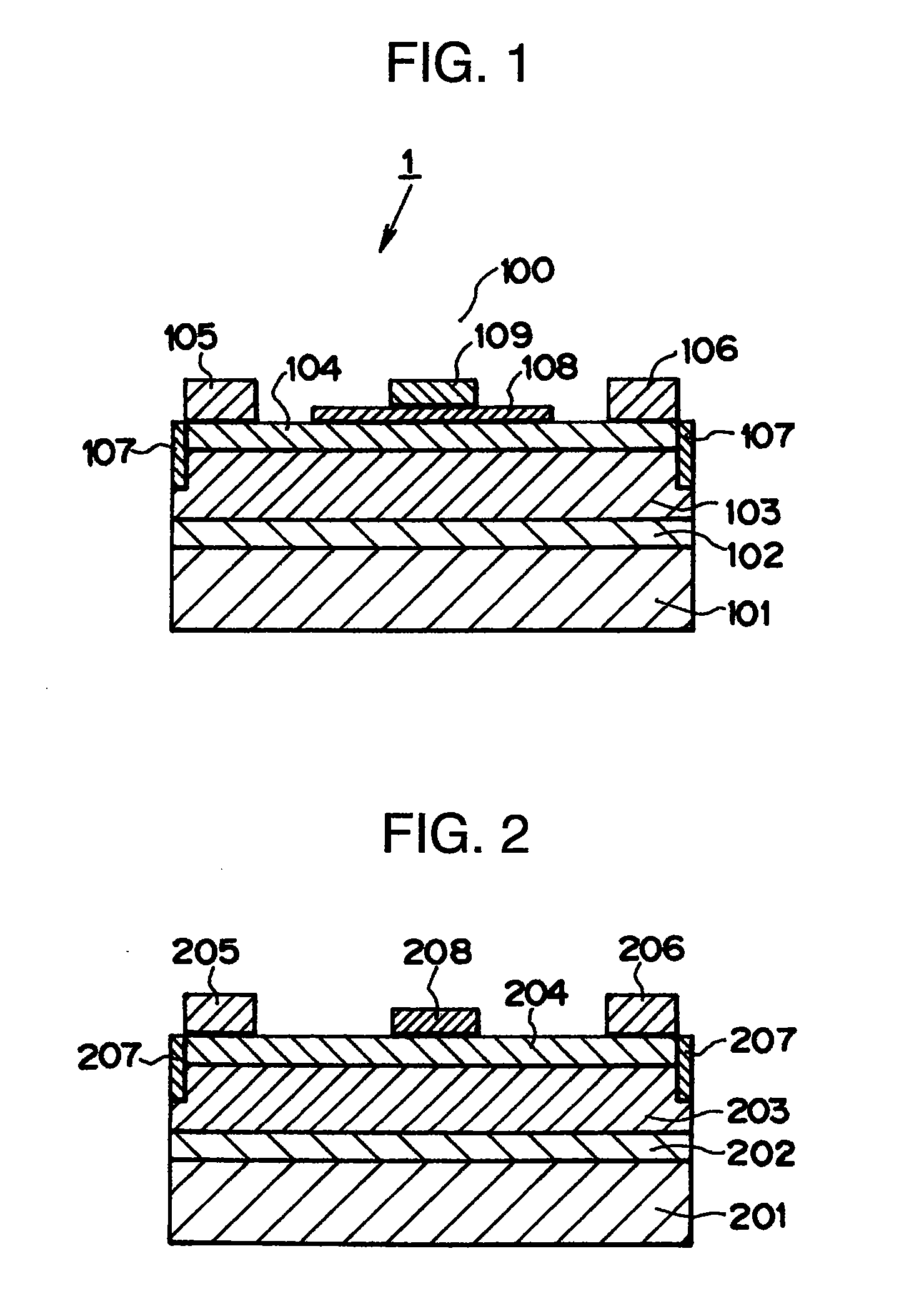
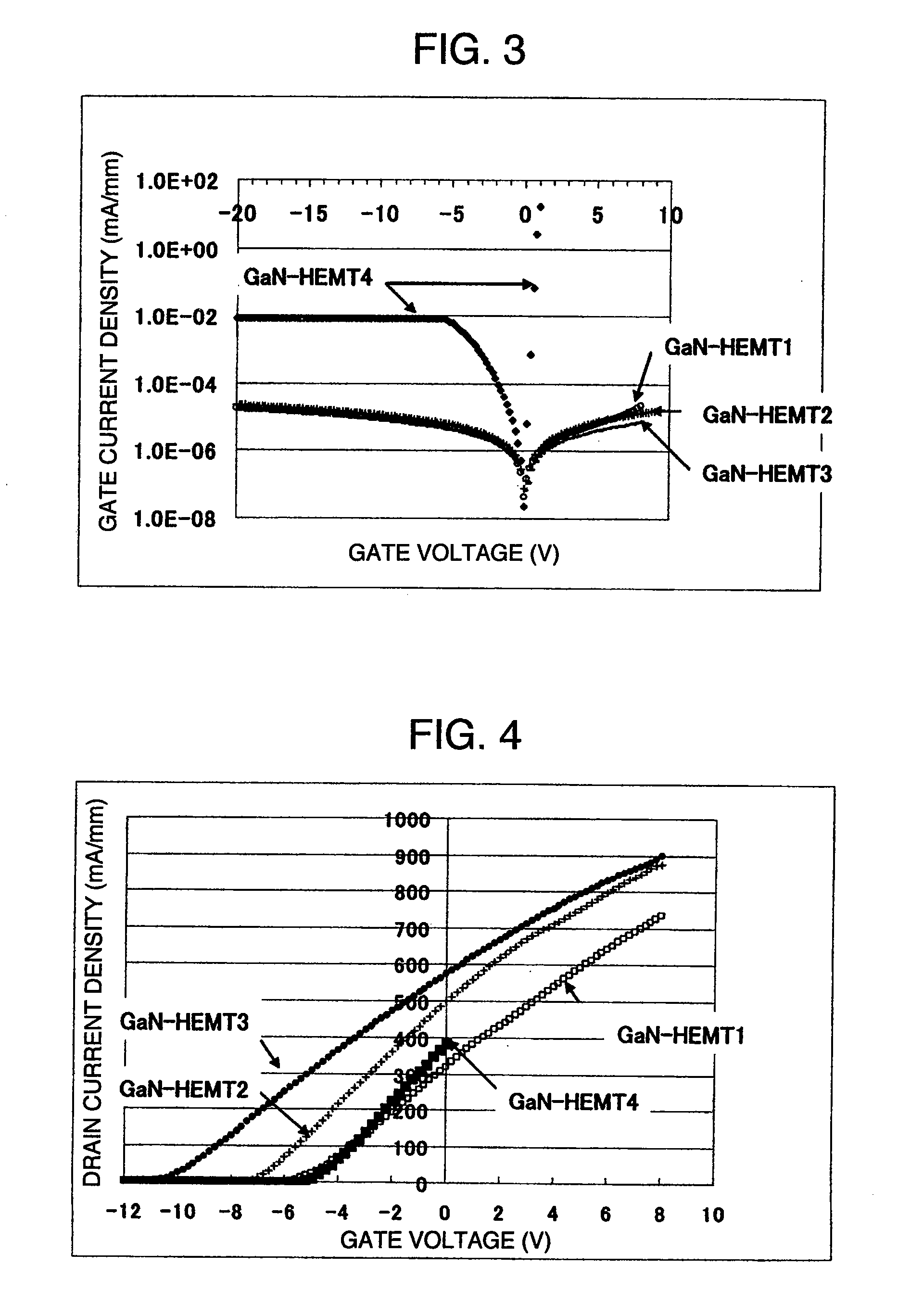
[0055]GaN-HEMTs having the configuration shown in FIG. 1 were fabricated as follows.

[0056]A semi-insulating SiC substrate 101 prepared as a base substrate 101 was washed with a mixture of sulfuric acid and hydrogen peroxide, and then heated to 600° C. in a MOCVD furnace. Thereafter, 40 sccm of TMA was supplied from a chamber under the following conditions: the temperature of the constant temperature tank; 30° C., and the flow rates of carrier gases of hydrogen and ammonia; 60SLM and 40SLM, respectively. Then, AlN was grown as a buffer layer 102 to a thickness of 500 Å.

[0057]Subsequently, the temperature of the base substrate 101 was changed to 1,150° C., and the flow rate of TMA was adjusted to 0 sccm. Then, 40 sccm of TMG was supplied from the constant temperature tank of 30° C., and a GaN layer was laminated on a buffer layer 102 as a semiconductor crystal layer 103 to a thickness of 2 μm.

[0058]Subsequently, the flow rate of TMG was changed to 100 sccm, and 3 sccm of TMA was suppl...


PUM


Abstract

A gallium nitride based field effect transistor having good current hysteresis characteristics in which forward gate leakage can be reduced. In a gallium nitride-based field effect transistor (100) having a gate insulation film (108), part or all of a material constituting the gate insulation film (108) is a dielectric material having a relative dielectric constant of 9-22, and a semiconductor crystal layer A (104) in contact with the gate insulation film (108) and a semiconductor crystal layer B (103) in the vicinity of the semiconductor crystal layer A (104) and having a larger electron affinity than the semiconductor crystal layer A (104) constitute a hetero junction. A hafnium oxide such as HfO2, HfAlO, HfAlON or HfSiO is preferably contained, at least partially, in the material constituting the gate insulation film (108).

Description

TECHNICAL FIELD[0001]The present invention relates to a semiconductor field effect transistor, a semiconductor integrated circuit and a method for fabricating the same.BACKGROUND ART[0002]Semiconductor field effect transistors are widely used as electronic components such as amplifiers or switches, and are classified into several categories depending on the forms of current pathway (channel). An example includes a field effect transistor utilizing a two-dimensional electron gas (2DEG). Such field effect transistors are divided into two types depending on the forms of the interfaces at which a 2DEG is formed. In the first type a 2DEG is formed at an oxide film / semiconductor crystal interface. In the second type a 2DEG is formed at a similar semiconductor crystal / semiconductor crystal interface. A representative example of the first type is a Si-MOS field effect transistor, and a representative example of the second type is a GaN high electron mobility field effect transistor (GaN-HEM...

Claims


Application Information

Patent Timeline
Patent Type & Authority Applications(United States)
IPC IPC(8): H01L29/04H01L21/336
CPCH01L29/2003H01L29/7783H01L29/517
Inventor SAZAWA, HIROYUKISHIMIZU, MITSUAKIYAGI, SHUICHIOKUMURA, HAJIME
Owner SUMITOMO CHEM CO LTD
Why Eureka
Try Eureka