Capacitor, semiconductor device comprising the same, method for manufacturing the capacitor, and method for manufacturing the semiconductor device

Inactive Publication Date: 2011-01-27
RENESAS ELECTRONICS CORP
View PDF3 Cites 22 Cited by
  • Summary
  • Abstract
  • Description
  • Claims
  • Application Information

AI Technical Summary

Benefits of technology

[0021]According to the present invention, it is possible to prevent the deterioration of electrical properties of the capacitor associated with the crystallization of a metal film that makes up the lower electrode and increase the permittivity of the capacitance insulation film. Even if elements are made smaller, it is possible to realize the capacitor having a sufficiently large capacitance with leakage current being reduced.

Problems solved by technology

For example, in the field of an advanced DRAM (Dynamic Random Access Memory) device, the shrinking of the size of a memory cell leads to a limited space occupancy for capacitors that make up a memory cell.
If the capacitors do not have enough capacitance, the memory cell is prone to malfunctioning as the electric charge of the capacitors decreases due to noise signals from the outside and the like.
Such malfunctions trigger errors, one typical example of which is a soft error.

Method used


Image

  • Capacitor, semiconductor device comprising the same, method for manufacturing the capacitor, and method for manufacturing the semiconductor device
  • Capacitor, semiconductor device comprising the same, method for manufacturing the capacitor, and method for manufacturing the semiconductor device
  • Capacitor, semiconductor device comprising the same, method for manufacturing the capacitor, and method for manufacturing the semiconductor device

Examples


example 1

[0135]Example 1 of the present invention will be described.

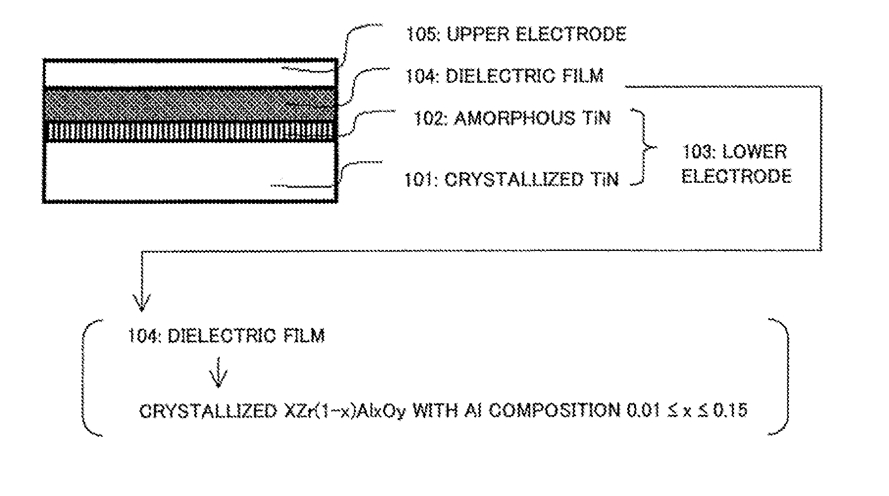
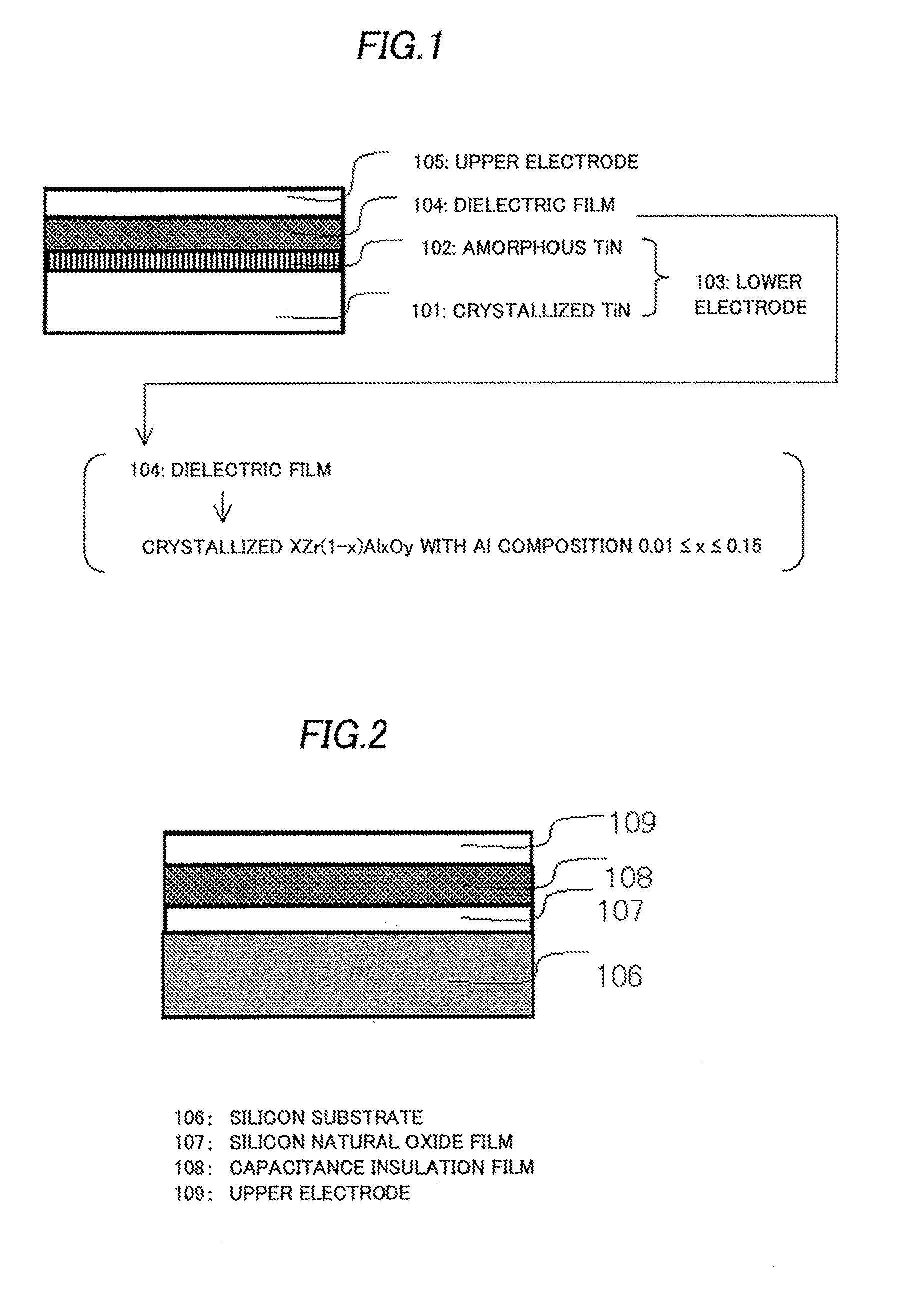
[0136]FIG. 10 is a diagram illustrating the cross-sectional structure of a capacitor, which is a semiconductor element, according to the present example. As shown in FIG. 10, on a silicon substrate 303 of the capacitor of the present example, a lower electrode 304, a metal-oxide-layer dielectric film 304 that makes up a capacitance insulation film, and an upper electrode 306 are formed. The lower electrode 304 is a laminated film made up of a lower-layer crystallized TiN 302 and an upper-layer amorphous TiN 303.

[0137]The following describes a method of producing the capacitor of the present example.

[0138]After the crystallized TiN 302 is deposited on the silicon substrate 301 with a thickness of 20 nm as part of the laminated structure of the lower electrode 304, the amorphous TiN 303 is formed with a thickness of 5 nm. The crystallized TiN film 302 can be made by a sputtering, chemical vapor deposition or ALD (Atomic Layer ...

example 2

[0151]Example 2 of the present invention will be described.

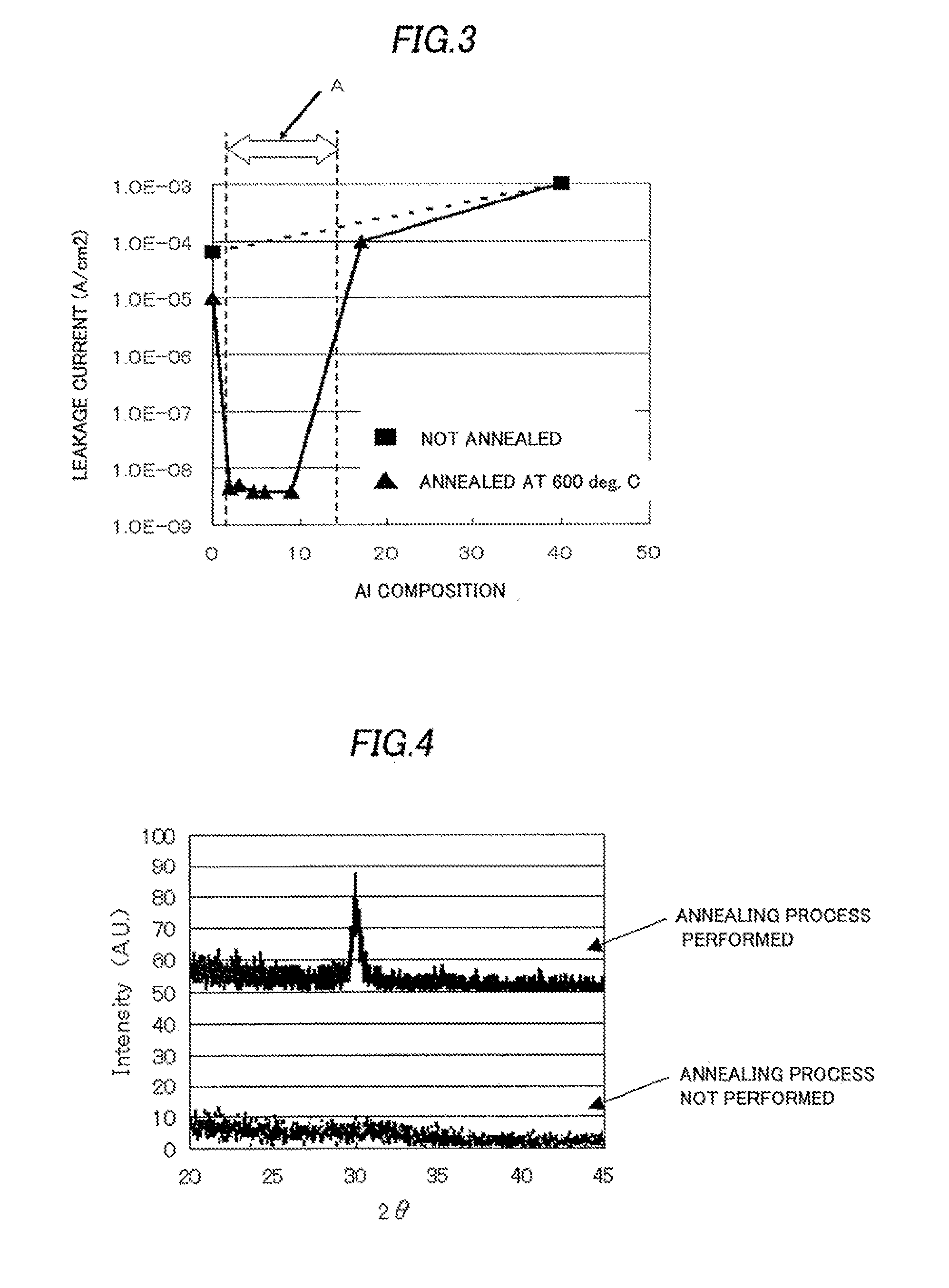
[0152]As for a method of producing a capacitor, which is a semiconductor element of the present example, in similar processes to those of Example 1, the Zr(1-x)AlxOy film is formed on an electrode with the Al composition x=0.045 and a thickness of 2 nm to 20 nm; an annealing process is performed for 10 minutes at 400 and 600 degrees Celsius under a nitrogen atmosphere. Then, Au is deposited on the Zr(1-x)AlxOy film by a vacuum deposition method with a film thickness of 100 nm to form a capacitor. The laminated electrode of the crystallized or amorphous TiN and the crystallized TiN serves as a first electrode, and the Au as a second electrode.

[0153]A voltage is applied to the first electrode of the formed capacitor; the EOT of the element is evaluated by CV measurements, and the leakage current by IV measurements. The results are that EOT=0.7 nm for the Zr(1-x)AlxOy film on the crystallized TiN and the leakage current is 1.5×...

example 3

[0156]Example 3 of the present invention will be described.

[0157]FIGS. 13 to 18 are cross-sectional diagrams showing the process sequence of a method of producing a semiconductor device having a capacitor, which is a semiconductor device of the present example.

[0158]First, as shown in FIG. 13A, an element isolation region 2 is formed by a LOCOS (Local Oxidation of Silicon) method or STI (Shallow Trench Isolation) method on the surface region of a p-type silicon substrate 1.

[0159]In an active region encircled by the element isolation region 2, a silicon oxide film and a polycrystalline silicon film are sequentially formed; with the use of a lithographic technique and RIE (Reactive Ion Etching) technique, the laminated film is processed into a desired shape to form a gate oxide film 3 and a gate electrode 4.

[0160]Then, ion implantation is conducted using the gate oxide film 3 and the gate electrode 4 as masks to introduce n-type impurities into the silicon substrate 1. A plurality of ...


PUM


Abstract

Provided is a capacitor that realizes a capacitance insulation film having a large relative permittivity and has sufficient capacitance even if an occupied space is small with a reduced amount of leakage current. A capacitor includes: a capacitance insulation film; and an upper electrode and lower electrode each formed on both sides of the capacitance insulation film. The capacitance insulation film is a complex oxide whose main ingredients are Zr, Al and O with the composition ratio of Zr to Al being set at (1−x): x (0.01≦x≦0.15) and is composed of a dielectric substance having a crystal structure. The lower electrode is composed of a conductor whose surface contiguous to at least the dielectric film has an amorphous structure.

Description

TECHNICAL FIELD[0001]The present invention relates to a capacitor, a semiconductor device having the capacitor, and a method of producing the capacitor and semiconductor device and particularly to a capacitor using a complex oxide film containing Zr and Al as a dielectric substance and a semiconductor device having the capacitor.BACKGROUND ART[0002]In the development of a semiconductor device, elements are further integrated; each element is made smaller and an operating voltage is reduced. For example, in the field of an advanced DRAM (Dynamic Random Access Memory) device, the shrinking of the size of a memory cell leads to a limited space occupancy for capacitors that make up a memory cell. If the capacitors do not have enough capacitance, the memory cell is prone to malfunctioning as the electric charge of the capacitors decreases due to noise signals from the outside and the like. Such malfunctions trigger errors, one typical example of which is a soft error.[0003]In general, th...

Claims


Application Information

Patent Timeline
IPC IPC(8): H01L27/08H01L21/02
CPCH01L21/02178H01L21/02189H01L21/02194H01L21/022H01L21/02271H01L28/40H01L21/3142H01L21/316H01L27/10811H01L27/10852H01L21/0228H10B12/312H10B12/033H01L21/02181
Inventor NAKAGAWA, TAKASHIMORI, KAORUIKARASHI, NOBUYUKIOSHIDA, MAKIKO
Owner RENESAS ELECTRONICS CORP
Why Eureka
Try Eureka