Method for forming microcrystalline semiconductor film and method for manufacturing thin film transistor

a technology of microcrystalline semiconductors and thin film transistors, applied in semiconductor devices, chemical vapor deposition coatings, coatings, etc., can solve the problems of poor electrical characteristics of thin film transistors, and achieve the effects of high crystallinity, small current, and large curren

Active Publication Date: 2011-01-27
SEMICON ENERGY LAB CO LTD
View PDF9 Cites 10 Cited by
  • Summary
  • Abstract
  • Description
  • Claims
  • Application Information

AI Technical Summary

Benefits of technology

[0007]In views of the above-mentioned problems, an object of one embodiment of the present invention is to form a microcrystalline semiconductor film having a high crystallinity. Another object of one embodiment of the present invention is to manufacture, with a high mass productivity, thin film transistors each having preferable electric characteristics and a high reliability and a display devices including the thin film transistors.
[0009]According to one embodiment of the present invention, a deposition gas containing silicon or germanium is constantly introduced into a treatment chamber while a flow ratio of hydrogen to the deposition gas containing silicon or germanium is periodically changed, and high-frequency power is supplied, whereby a step in which crystal nuclei are generated, a step in which the crystal nuclei are grown, and a step in which an amorphous portion of a deposition surface is etched are repeated. The growth of the crystal nuclei is performed while the density of the crystal nuclei is increased; therefore, a microcrystalline semiconductor film having a high crystallinity can be formed.
[0019]When the deposition gas containing silicon or germanium is introduced into a treatment chamber while the flow ratio of hydrogen to the deposition gas containing silicon or germanium is periodically changed, the size of a crystallite included in a crystal grain can be increased, and thus, a microcrystalline semiconductor film having a high crystallinity can be formed.
[0020]When a deposition gas containing silicon or germanium is introduced into a treatment chamber while a flow ratio of hydrogen to the deposition gas containing silicon or germanium is periodically changed and the flow rate of a rare gas is periodically changed, the size of a crystallite included in a crystal grain can be increased and crystal grains can adjoin; therefore, a microcrystalline semiconductor film having a high crystallinity can be formed.
[0024]As described above, a thin film transistor having a high crystallinity can be formed. Further, a thin film transistor with small off current and large on current can be manufactured with high productivity.

Problems solved by technology

An inversed staggered thin film transistor in which a microcrystalline semiconductor film is used for a channel formation region has problems in that the microcrystalline semiconductor film has a low crystallinity at an interface region between a gate insulating film and the microcrystalline semiconductor film and electric characteristics of the thin film transistor are poor.

Method used


Image

  • Method for forming microcrystalline semiconductor film and method for manufacturing thin film transistor
  • Method for forming microcrystalline semiconductor film and method for manufacturing thin film transistor
  • Method for forming microcrystalline semiconductor film and method for manufacturing thin film transistor

Examples


embodiment 1

[0045]In this embodiment, a method for forming a microcrystalline semiconductor film having a high crystallinity is described with reference to FIG. 1 and FIG. 2.

[0046]In this embodiment, a crystalline semiconductor film is formed by glow discharge plasma using a mixture of a deposition gas containing silicon or germanium and hydrogen in a treatment chamber of a plasma CVD apparatus. Here, the flow rate of hydrogen is fixed and the flow rate of the deposition gas containing silicon or germanium is controlled with time; thus, a microcrystalline semiconductor film having a high crystallinity is formed.

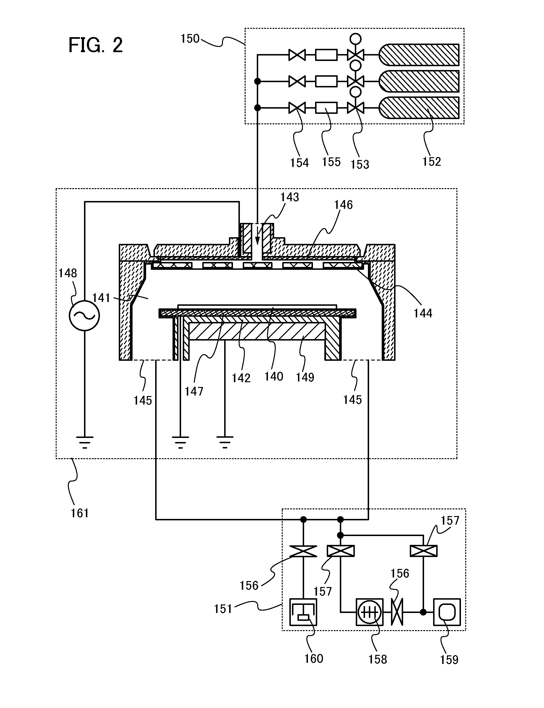
[0047]First, one mode of a plasma CVD apparatus which is used in this embodiment is described with reference to FIG. 2.

[0048]A plasma CVD apparatus 161 illustrated in FIG. 2 is connected to a gas supply unit 150 and an exhaust unit 151 and includes a treatment chamber 141, a stage 142, a gas supply portion 143, a shower plate 144, an exhaust port 145, an upper electrode 146, a lower elec...

embodiment 2

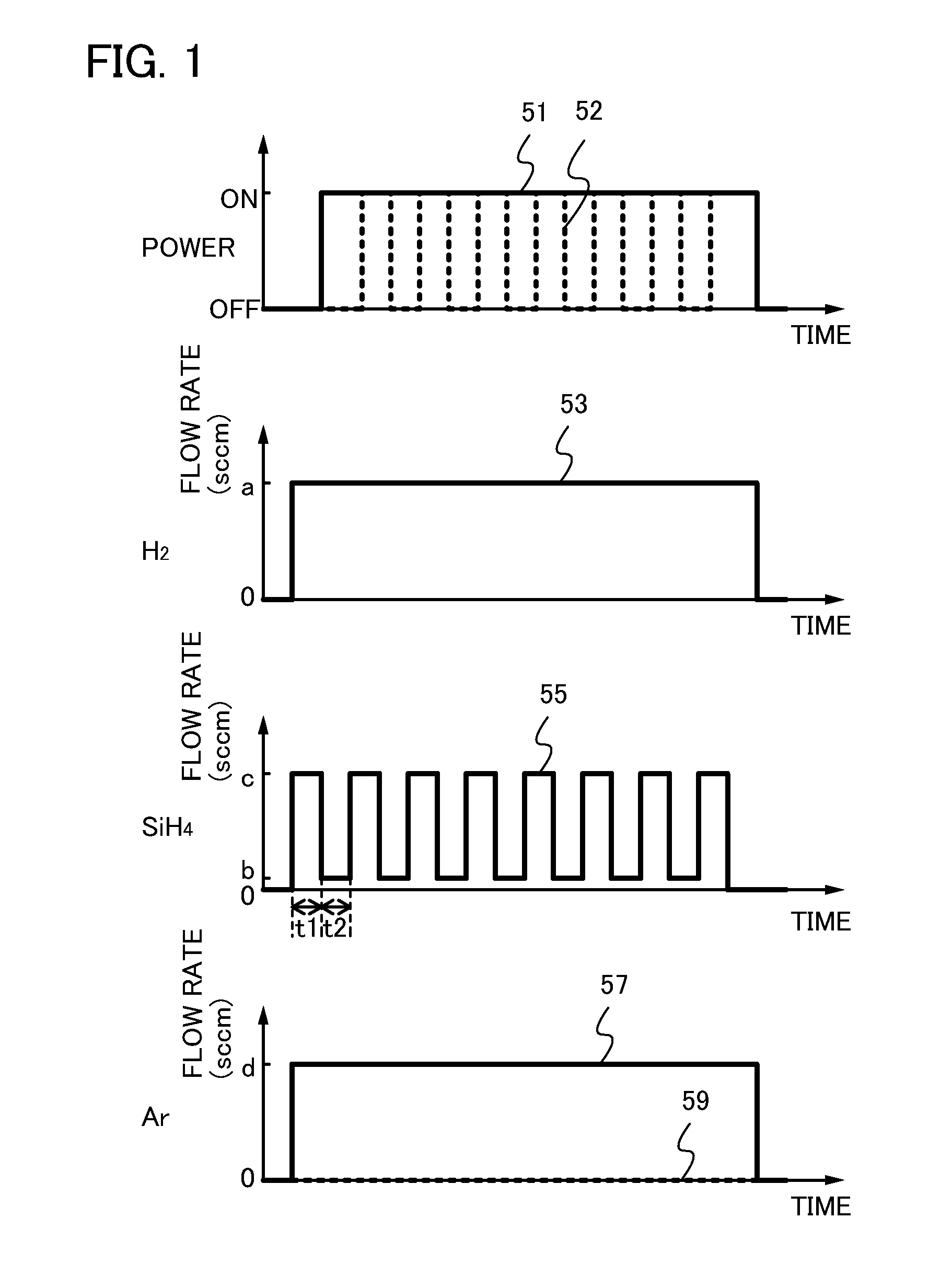
[0069]In this embodiment, a method for forming a microcrystalline semiconductor film having a high crystallinity in which crystal grains are adjacent to each other is described with reference to FIG. 3.

[0070]FIG. 3 shows timing charts each illustrating temporal changes in a source gas in a method for forming a microcrystalline semiconductor film described in this embodiment. In FIG. 3, a solid line 61 indicates on / off states of power supply of the plasma CVD apparatus, a solid line 63 indicates the flow rate of hydrogen, a solid line 65 indicates the flow rate of the deposition gas containing silicon or germanium (silane is used in FIG. 3), and a solid line 67 indicates the flow rate of a rare gas (argon is used in FIG. 3).

[0071]A deposition gas containing silicon or germanium, which is a source gas, and hydrogen are introduced into the treatment chamber of the plasma CVD apparatus and the pressure therein is set at a predetermined level. The temperature of the substrate 140 is set ...

embodiment 3

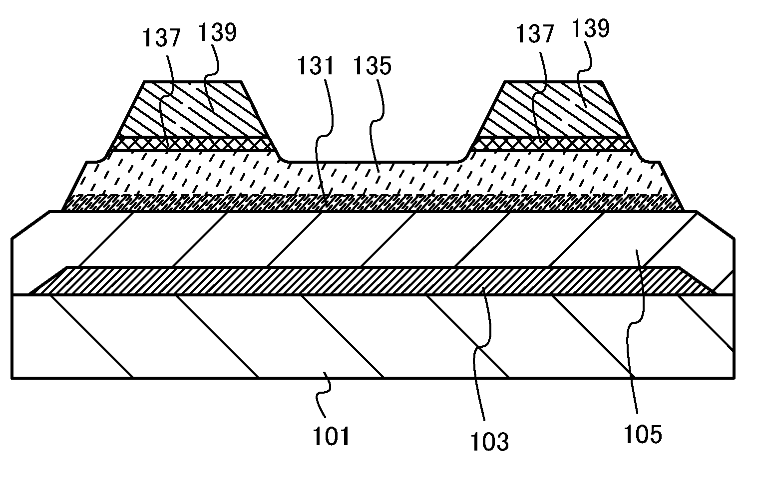
[0080]In this embodiment, structures of a thin film transistor including a microcrystalline semiconductor film formed by any of the methods described in Embodiments 1 and 2 are described with reference to FIGS. 4A to 4C.

[0081]A microcrystalline semiconductor film formed by any of the methods described in Embodiments 1 and 2 can be used as a channel formation region in a thin film transistor. Although the microcrystalline semiconductor film can be used in both a bottom gate thin film transistor and a top gate thin film transistor, the microcrystalline semiconductor film can improve characteristics of the bottom gate thin film transistor particularly. Here, a typical structure of the bottom gate thin film transistor is described with reference to FIGS. 4A to 4C.

[0082]A thin film transistor illustrated in FIG. 4A is a channel etched thin film transistor. A gate electrode 103 is formed over a substrate 101 and a gate insulating film 105 is formed to cover the substrate 101 and the gate ...


PUM

PropertyMeasurementUnit
pressureaaaaaaaaaa
sizesaaaaaaaaaa
sizesaaaaaaaaaa

Abstract

A microcrystalline semiconductor film having a high crystallinity is formed. Further, a thin film transistor having preferable electric characteristics and high reliability and a display device including the thin film transistor are manufactured with high mass productivity. A step in which a deposition gas containing silicon or germanium is introduced at a first flow rate and a step in which the deposition gas containing silicon or germanium is introduced at a second flow rate are repeated while hydrogen is introduced at a fixed rate, so that the hydrogen and the deposition gas containing silicon or germanium are mixed, and a high-frequency power is supplied. Therefore, a microcrystalline semiconductor film is formed over a substrate.

Description

BACKGROUND OF THE INVENTION[0001]1. Field of the Invention[0002]The present invention relates to a microcrystalline semiconductor film, a thin film transistor, and methods for manufacturing the microcrystalline semiconductor film and the thin film transistor. The present invention also relates to a display device to which the thin film transistor is applied.[0003]2. Description of the Related Art[0004]As a kind of field-effect transistor, a thin film transistor in which a channel formation region is formed in a semiconductor film formed over a substrate having an insulating surface is known. Techniques for using microcrystalline silicon for semiconductor films used in thin film transistors have been disclosed (see Patent Documents 1 to 4). A typical application of the thin film transistor is a liquid crystal television device in which the thin film transistor has been put to practical use as a switching transistor for a pixel that constitutes a display screen.REFERENCE[Patent Docume...

Claims


Application Information

Patent Timeline
Patent Type & Authority Applications(United States)
IPC IPC(8): H01L21/336H01L21/20
CPCC23C16/24C23C16/28C23C16/45523H01L21/02422H01L29/78684H01L21/02595H01L21/0262H01L29/78669H01L29/78678H01L21/02532
Inventor TAJIMA, RYOTATANAKA, TETSUHIROTOKUMARU, RYOMIYAIRI, HIDEKAZUICHIJO, MITSUHIRONOZAWA, TAICHI
Owner SEMICON ENERGY LAB CO LTD
Why Eureka
Try Eureka