
Target, method for producing the same, memory, and method for producing the same

a technology of target and memory, which is applied in the direction of transportation and packaging, vacuum evaporation coating, coating, etc., can solve the problems of difficult simultaneous dissolution of constituent elements, difficult to form a target by dissolution methods, etc., and achieve the effect of less danger of ignition, less risk of ignition, and reduced number of cathodes in the film formation apparatus for forming an ionization layer of memory devices

Inactive Publication Date: 2011-02-03
SONY CORP
View PDF1 Cites 12 Cited by
  • Summary
  • Abstract
  • Description
  • Claims
  • Application Information

AI Technical Summary

Benefits of technology

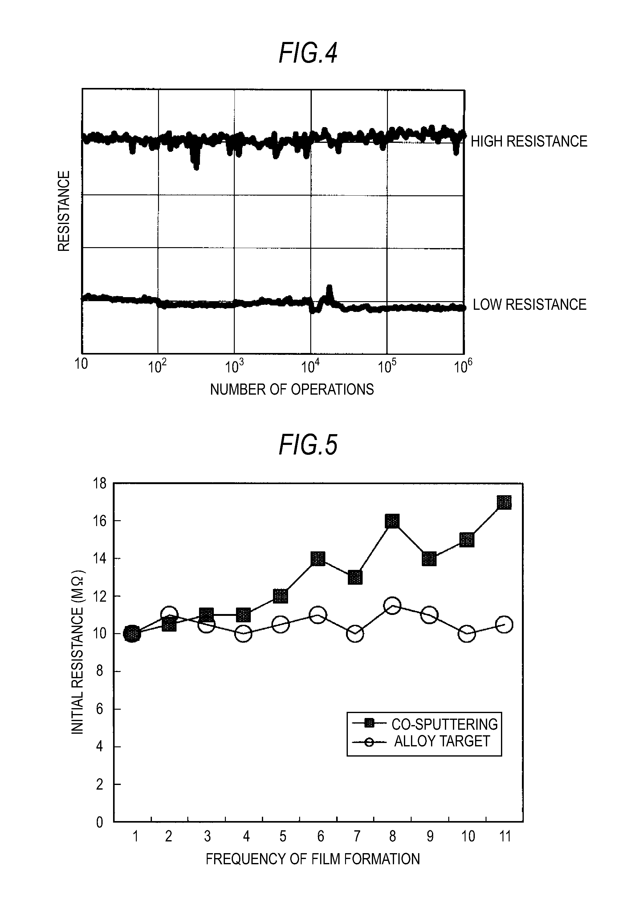
[0020]However, in order to improve the uniformity of composition of ionization layers and reduce the variation among wafers, it is preferable that the ionization layers are formed using one target.
[0045]Further, the variation in composition or thickness among wafers, which is often observed in the case of co-sputtering or periodical stacking, can also be reduced.

Problems solved by technology

Accordingly, it is difficult to simultaneously dissolve the constituent elements, and it thus is difficult to form a target by a dissolution method.

Method used


Image

  • Target, method for producing the same, memory, and method for producing the same
  • Target, method for producing the same, memory, and method for producing the same
  • Target, method for producing the same, memory, and method for producing the same

Examples


experimental examples

3. Experimental Examples

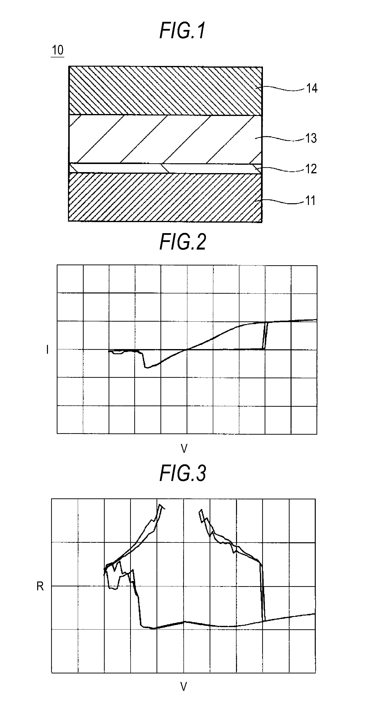
[0136]A target was actually produced, and a memory including memory devices was produced using the target.

[0137]With respect to the memory, the characteristics of its memory devices were examined.

example 1

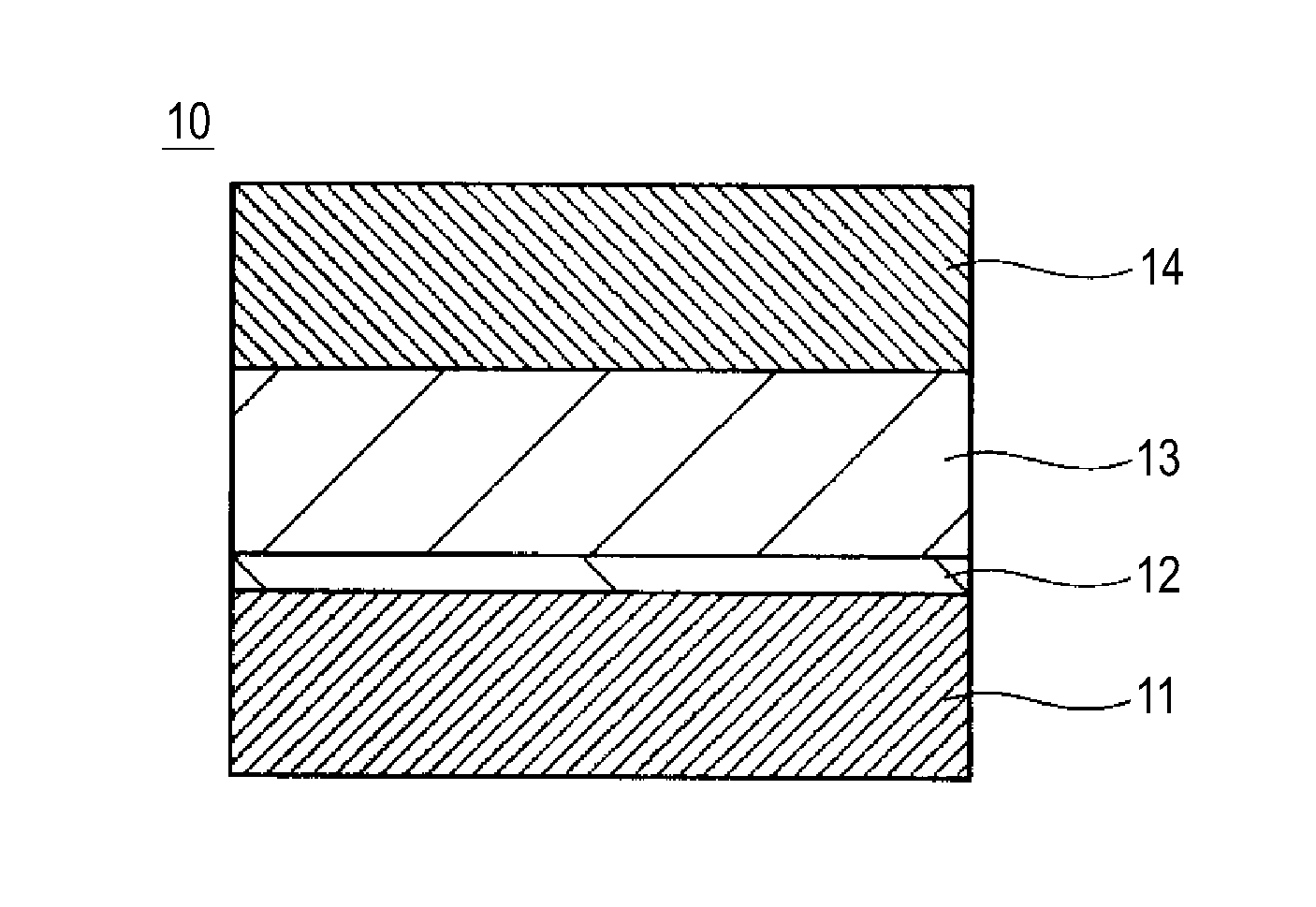
[0138]First, using a 1-mm3 Zr scrap as a Zr raw material of the group of refractory metal elements M1, 1-cm3 Al pellets and a 3-cm2 Cu thin plat as raw materials of the group of elements M2 were dissolved in a high-frequency melting furnace to prepare an AlCuZr alloy ingot.

[0139]Subsequently, the alloy ingot was pulverized in an attritor to prepare an alloy powder with a particle diameter of 106 Ωm or less.

[0140]Subsequently, the alloy powder was mixed with a Te powder with a particle diameter of 75 μm or less and a Ge power with a particle diameter of 32 to 106 μm, and the mixture was sintered to give an AlCuGeTeZr target base material.

[0141]The target base material was then cut into a disc-like piece with a thickness of 5 mm and a diameter of 300 mm to give a target.

[0142]The prepared target was adhered to the backing plate of a sputtering apparatus using In wax.

[0143]Subsequently, a Gd oxide film with a thickness of 2 nm was formed as a high resistance layer 12 on a CMOS circuit ...

example 2

[0154]Using a 1-mm3 Zr scrap as a Zr raw material of the group of refractory metal elements M1, an Al powder as an Al raw material of the group of elements M2 was mixed and dissolved in a high-frequency melting furnace to prepare an AlZr alloy ingot. The prepared alloy ingot was pulverized to give an alloy powder.

[0155]Subsequently, Ge, Cu, and Te raw materials were dissolved in a high-frequency melting furnace to prepare an alloy ingot, which was then pulverized to give an alloy powder.

[0156]These two kinds of alloy powders were then mixed at a desired composition ratio, and sintered to give an AlCuGeTeZr target base material.

[0157]The target base material was then cut into a disc-like piece with a thickness of 5 mm and a diameter of 300 mm to give a target.

[0158]Then, in the same manner as in Example 1, a memory cell array having a large number of memory devices 10 was formed on a wafer to give a sample of the memory of Example 2.

[0159]The characteristics of the memory of the samp...


PUM

PropertyMeasurementUnit
Particle diameteraaaaaaaaaa
Melting pointaaaaaaaaaa

Abstract

A target includes: at least one refractory metal element selected from the group consisting of Ti, Zr, Hf, V, Nb, Ta, and lanthanoids; at least one element selected from the group consisting of Al, Ge, Zn, Co, Cu, Ni, Fe, Si, Mg, and Ga; and at least one chalcogen element selected from the group consisting of S, Se, and Te.

Description

BACKGROUND OF THE INVENTION[0001]1. Field of the Invention[0002]The present invention relates to a target containing a refractory metal element and a chalcogen element and to a method for producing the same. The invention also relates to a memory including a memory device having an ionization layer formed using a target and to a method for producing the same.[0003]2. Description of the Related Art[0004]A high-speed, high-density DRAM has been widely used as a random access memory in an information-processing apparatus, such as a computer.[0005]However, DRAMs are volatile memories that lose their contents when the power is turned off, and the written information (data) has to be frequently refreshed, i.e., the data needs to be frequently read, reamplified, and rewritten.[0006]As non-volatile memories that do not lose their contents when the power is turned off, a flash memory, an FeRAM (ferroelectric random-access memory), an MRAM (magnetic memory device), and the like have been prop...

Claims


Application Information

Patent Timeline
IPC IPC(8): B32B15/04C23C14/34C22C1/10C22C1/04
CPCB22F9/04C22C1/05C23C14/3414H01L45/085H01L45/1233H01L45/1625H01L45/145H01L45/146C23C14/14H01L45/08H01L45/1266Y10T428/31678H10N70/245H10N70/8416H10N70/011H10N70/826H10N70/8833C23C14/3407H10N70/883H10N70/24H10N70/026H10N70/882
Inventor OHBA, KAZUHIROKAMORI, YUICHIKIMURA, HITOSHI
Owner SONY CORP
Learn More