Method for making a full-spectrum solar cell with an anti-reflection layer doped with silicon quantum dots

a solar cell and anti-reflection technology, applied in the field of full-spectrum solar cells, can solve the problems of small penetration depth of photons, damage to solar cells, and electron-hole pairs caused by photons that are easy to be captured superficially

Inactive Publication Date: 2011-02-03
INST NUCLEAR ENERGY RES ROCAEC
View PDF5 Cites 13 Cited by
  • Summary
  • Abstract
  • Description
  • Claims
  • Application Information

AI Technical Summary

Benefits of technology

[0007]It is another objective of the present invention to provid...

Problems solved by technology

The portion of the energy of photons higher than the band gap will become heat that would damage the solar cell.
Moreover, the penetration dep...

Method used


Image

  • Method for making a full-spectrum solar cell with an anti-reflection layer doped with silicon quantum dots
  • Method for making a full-spectrum solar cell with an anti-reflection layer doped with silicon quantum dots
  • Method for making a full-spectrum solar cell with an anti-reflection layer doped with silicon quantum dots

Examples


first embodiment

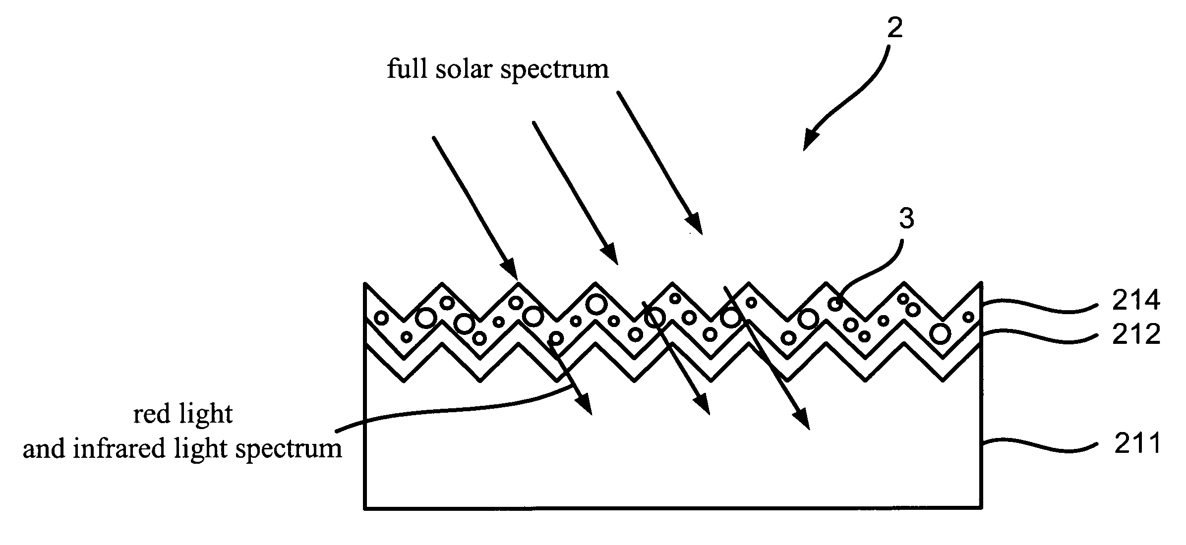
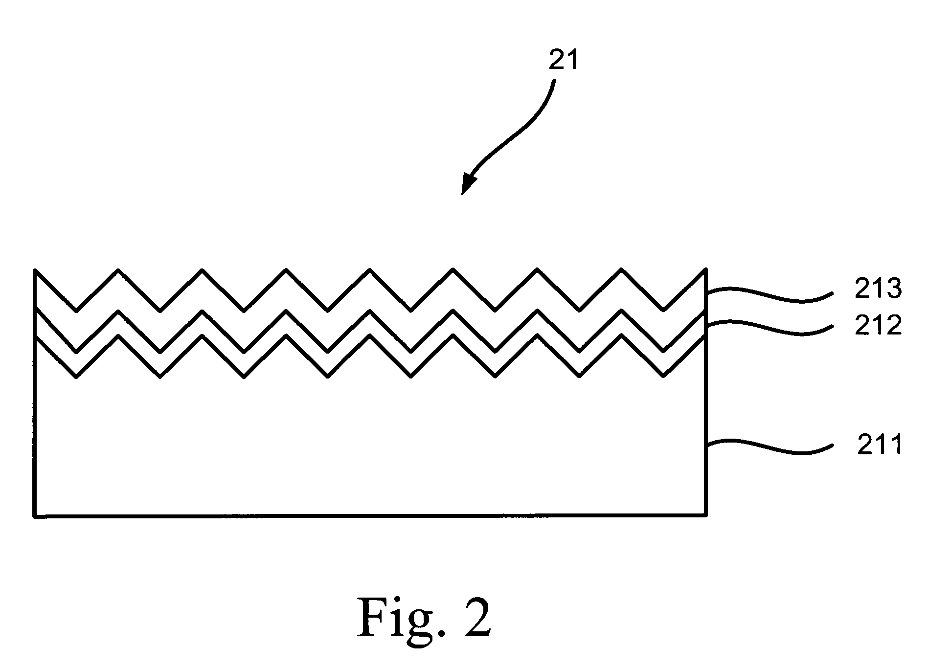
[0022]Referring to FIGS. 1 and 2, at 11, a single-crystal solar cell 21 is provided according to the present invention. The single-crystal solar cell 21 includes a p-type substrate 211, an n-type diffusion layer 212 and an anti-reflection layer 213.

[0023]Referring to FIGS. 1 and 3, at 12, the anti-reflection layer 213 is transformed into an anti-reflection layer 214 doped with silicon quantum dots 3 based on a physical or chemical method. Such a method is plasma-enhanced chemical vapor deposition, electron cyclotron resonance chemical vapor deposition, very high frequency chemical vapor deposition, hot wire chemical vapor deposition, e-gun or sputtering for example.

[0024]At first, the anti-reflection layer 213 is coated with a film of silicon nitride and / or silicon oxide. To this end, silicon hydride and dichlorosilane are used as a source of silicon, and nitrogen and ammonia are used as a source of nitrogen, and oxygen and nitrous oxide are used as a source of oxygen. The silicon / n...

second embodiment

[0028]Referring to FIG. 5, according to the present invention, there is provided a multi-crystal silicon solar cell 51 as the conventional solar cell. The multi-crystal silicon solar cell 51 includes a p-type substrate 511, an n-type diffusion layer 512 and an anti-reflection layer 513.

[0029]Referring to FIGS. 6 and 7, the anti-reflection layer 513 is transformed into an anti-reflection layer 514 doped with silicon quantum dots 6 later. For the transformation, the silicon / nitrogen ratio is higher than 3:4 while the silicon / oxygen ratio is higher than 1:2. The multi-crystal silicon solar cell 51 is transformed into a full-spectrum solar cell 5 including the anti-reflection layer 513 doped with the silicon quantum dots 6.

third embodiment

[0030]Referring to FIG. 8, according to the present invention, there is provided a thin-film silicon-based solar cell 71 as the conventional solar cell. The thin-film silicon-based solar cell 71 includes a substrate 711, a p-type layer 712, an i-type layer 713, an n-type layer 714 and an anti-reflection layer 715.

[0031]Referring to FIGS. 9 and 10, the anti-reflection layer 715 is transformed into an anti-reflection layer 716 doped with silicon quantum dots 8. For the transformation, the silicon / nitrogen ratio is higher than 3:4 while the silicon / oxygen ratio is higher than 1:2. The thin-film silicon-based solar cell 71 is transformed into a full-spectrum solar cell 7 including the anti-reflection layer 716 doped with the silicon quantum dots 8.


PUM


Abstract

In a method for making a full-spectrum solar cell, there is provided an ordinary solar cell with an anti-reflection layer. The anti-reflection layer is coated with a film of silicon nitride and/or silicon oxide. The silicon/nitrogen ratio and/or the silicon/oxygen ratio and the temperature are regulated, thus forming a silicon-rich film via doping the anti-reflection layer with silicon from the film of silicon nitride and/or silicon oxide. The precipitation of the silicon in the silicon-rich film is executed based on a mechanism of phase separation, thus forming silicon quantum dots of various sizes in the anti-reflection layer.

Description

BACKGROUND OF INVENTION[0001]1. Field of Invention[0002]The present invention relates to a method for making a full-spectrum solar cell and, more particularly, to a method for making a full-spectrum solar cell with an anti-reflection layer doped with silicon quantum dots.[0003]2. Related Art[0004]Conventional crystalline silicon solar cells and thin-film silicon-based solar cells include III-V group compound solar cells and II-VI group compound solar cells. Such a solar cell includes an anti-reflection layer. To make such the anti-reflection layer of a thin-film silicon-based solar cell, silicon nitride and / or silicon oxide are used. The silicon nitride is generally Si3N4 while the silicon oxide is SiO2. The band gap of such a silicon-based material is about 1.1 to 1.2 eV. The portion of the energy of photons higher than the band gap will become heat that would damage the solar cell. Moreover, the penetration depth of the photons is small so that electron-hole pairs caused by the ph...

Claims


Application Information

Patent Timeline
IPC IPC(8): H01L31/18
CPCH01L31/02168H01L31/0296H01L31/0322H01L31/068H01L31/0693Y02E10/547H01L31/0735Y02E10/541Y02E10/543Y02E10/544H01L31/073Y02P70/50
Inventor YANG, TSUN-NENG
Owner INST NUCLEAR ENERGY RES ROCAEC
Why Eureka
Try Eureka