Compound for organic thin-film transistor and organic thin-film transistor using the compound

a technology of organic thin film transistors and compound compounds, which is applied in the direction of organic chemistry, chemistry apparatus and processes, and the production of tft using such silicon by cvd apparatuses which are very expensive, and achieves the effect of high response speed (driving speed)

Inactive Publication Date: 2011-02-10
IDEMITSU KOSAN CO LTD
View PDF2 Cites 2 Cited by
  • Summary
  • Abstract
  • Description
  • Claims
  • Application Information

AI Technical Summary

Benefits of technology

[0023]The invention can provide a compound for an organic thin film transistor which is suited to a coating process.
[0024]By using the compound for an organic thin film transistor according to the invention as an organic semiconductor layer, an organic thin film transistor which has a high response speed (driving speed) can be provided.
[0025]The compound for an organic thin film transistor according to the invention can al

Problems solved by technology

However, a CVD apparatus which is used for production of the TFT using such silicon is very expensive, and to enlarge a display apparatus or the like using TFTs had a problem of significant increase in the production costs.
Further, the process of making the amorphous or polycrystalline silicon into a film is carried out at a very high temperature so that materials usable for a substrate are limited.
Thus, there is a problem that a lightweight substrate such as a resin substrate cannot be used.
However, the above-mentioned conventional compou

Method used


Image

  • Compound for organic thin-film transistor and organic thin-film transistor using the compound
  • Compound for organic thin-film transistor and organic thin-film transistor using the compound
  • Compound for organic thin-film transistor and organic thin-film transistor using the compound

Examples


example 1

Fabrication of Organic Thin Film Transistor

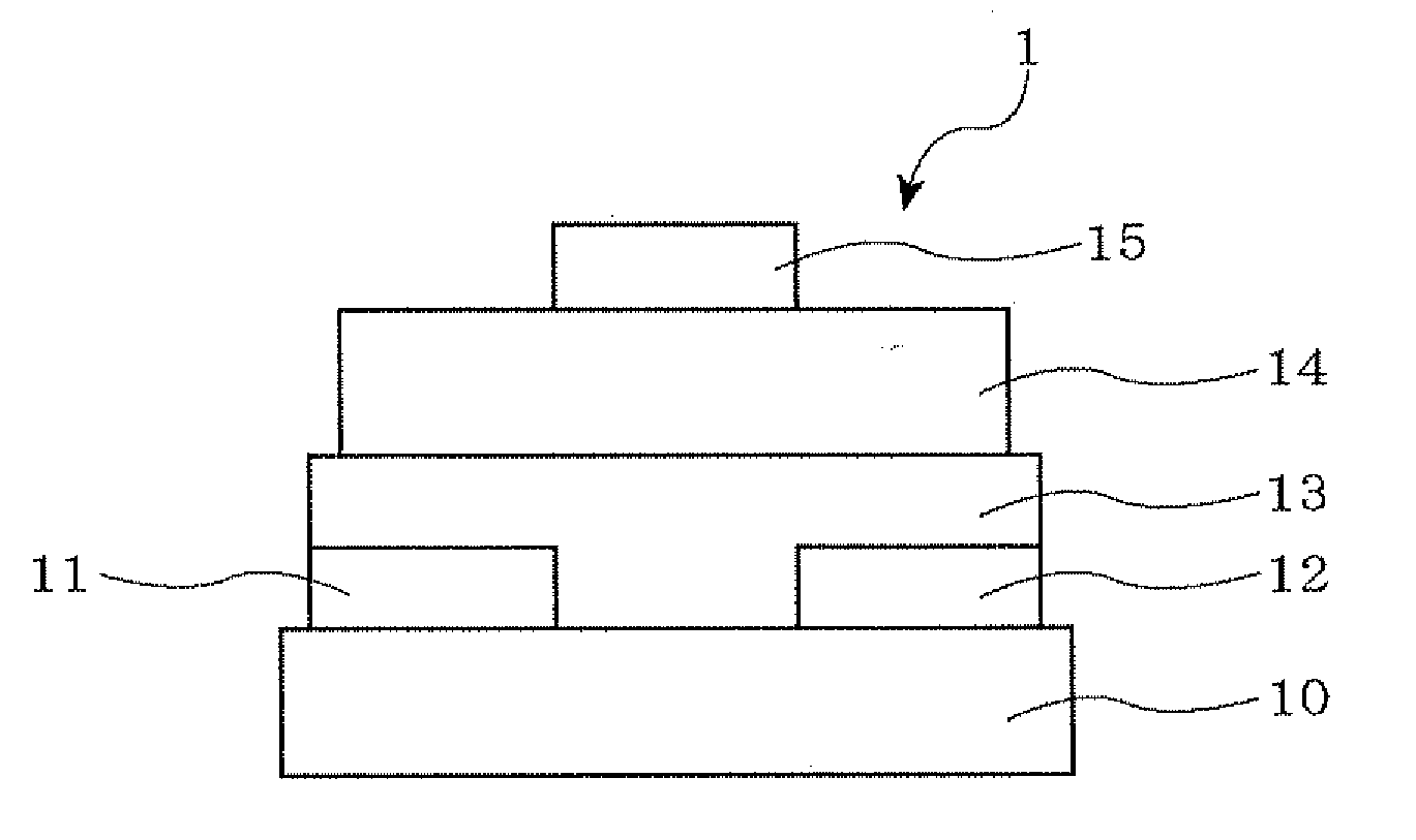
[0133]An organic thin film transistor as shown in FIG. 3 was fabricated in the following procedure. First, a glass substrate was subjected to ultrasonic cleaning with a neutral detergent, pure water, acetone and ethanol each for 30 minutes. Subsequently, gold (Au) was formed into a thin film having a thickness of 40 nm by sputtering to form a gate electrode. Then, the substrate was placed in a film-forming section of a thermal CVD reactor. On the other hand, to an evaporation section of a raw material, 250 mg of poly(p-xylene) derivative [poly(p-xylene) chloride (Parylene)] (Tradename: diX-C, manufactured by Daisan Kasei Co., Ltd.) which was the material for an insulating layer, which was put in a petri dish, was placed. The thermal CVD reactor was vacuated by a vacuum pump to a reduced pressure of 5 Pa. Subsequently, the evaporation section was heated up to a temperature of 180° C., a polymerization section up to a temperature of 680° C., ...

examples 2 and 3

Fabrication of Organic Thin Film Transistor

[0138]An organic thin film transistor was fabricated in the same manner as in Example 1 except that Compound (A-3) and Compound (A-5) was used in place of Compound (A-2) as a material for the organic semiconductor layer. In the same manner as in Example 1, the resultant organic thin film semiconductor was p-type driven at a gate voltage VG of −40 V. The on / off ratio of the current between the source-drain electrodes was measured, and the field effect mobility μ of holes was calculated. The results are shown in Table 1.

example 4

Fabrication of Organic Thin Film Transistor

[0139]In the same manner as in Example 1, cleaning of a substrate, formation of a gate electrode and formation of an insulating layer were carried out. Next, the substrate was placed in a vacuum deposition apparatus (manufactured by ULVAC, EX-400), and Compound (A-5) was deposited on the insulating layer at a deposition rate of 0.05 m / s to form a film having a thickness of 50 nm as an organic semiconductor layer. Then, by means of a vacuum vapor deposition apparatus, gold (Au) was deposited thereon through a metal mask into a film having a thickness of 50 nm to provide a source electrode and a drain electrode which did not contact each other, whereby an organic thin film transistor was fabricated.

[0140]In the same manner as in Example 1, the resultant organic thin film semiconductor was p-type driven at a gate voltage VG of −40 V. The on / off ratio of the current between the source-drain electrodes was measured, and the field effect mobility...


PUM

PropertyMeasurementUnit
Work functionaaaaaaaaaa
Areaaaaaaaaaaa

Abstract

A compound for an organic thin film transistor having a structure shown by the following formula (1):
X1-L-Ar-L-X2   (1)
wherein L is —C≡C—, or —CH═CH— in a trans configuration, X1 and X2 are independently an alkyl group having 2 to 30 carbon atoms or a haloalkyl group having 1 to 30 carbon atoms, and Ar is a substituted or unsubstituted aromatic hydrocarbon group having 14 to 60 ring carbon atoms which is a condensed ring of three or more rings, or a substituted or unsubstituted aromatic heterocyclic group having 11 to 60 ring atoms which is a condensed ring of three or more rings.

Description

TECHNICAL FIELD[0001]The invention relates to a compound suited to a coating process, a compound for an organic thin film transistor and an organic thin film transistor using the compound in an organic semiconductor layer.BACKGROUND ART[0002]Thin film transistors (TFTs) are widely used as a switching element for a display such as a liquid crystal display device. The representative TFT has a gate electrode, an insulating layer and an organic semiconductor layer on a substrate sequentially and has a source electrode and a drain electrode formed on the organic semiconductor layer with a predetermined distance. The organic semiconductor layer forms a channel region, and an electric current flowing between the source electrode and the drain electrode is controlled by applying a voltage to the gate electrode to allow the on / off action.[0003]Heretofore, the TFT has been made of amorphous silicon or polycrystalline silicon. However, a CVD apparatus which is used for production of the TFT us...

Claims


Application Information

Patent Timeline
IPC IPC(8): H01L51/10C07C13/62C07C13/66C07C13/573C07C22/08C07D333/78C07D495/04C07D495/14C07D513/04C07D493/04
CPCC07C15/56H01L51/0545C07C15/62C07C22/08C07C2103/24C07C2103/44C07C2103/52C07D333/76C07D493/04C07D495/04C07D495/14C07D513/04H01L51/0052H01L51/0541C07C15/60C07C2603/24C07C2603/44C07C2603/52H10K85/615H10K10/464H10K10/466
Inventor SAITO, MASATOSHINAKANO, YUKINAKAMURA, HIROAKI
Owner IDEMITSU KOSAN CO LTD
Why Eureka
Try Eureka