

Memory
a memory and dielectric layer technology, applied in the field of memory, can solve the problems of adversely affecting the performance of flash memory units, the thickness of the gate dielectric layer cannot be reduced proportionally, etc., and achieve the effect of raising the data storage and holding capability and reducing the size of the memory
- Summary
- Abstract
- Description
- Claims
- Application Information
AI Technical Summary
Benefits of technology
Problems solved by technology
Method used
Image

Examples
first embodiment
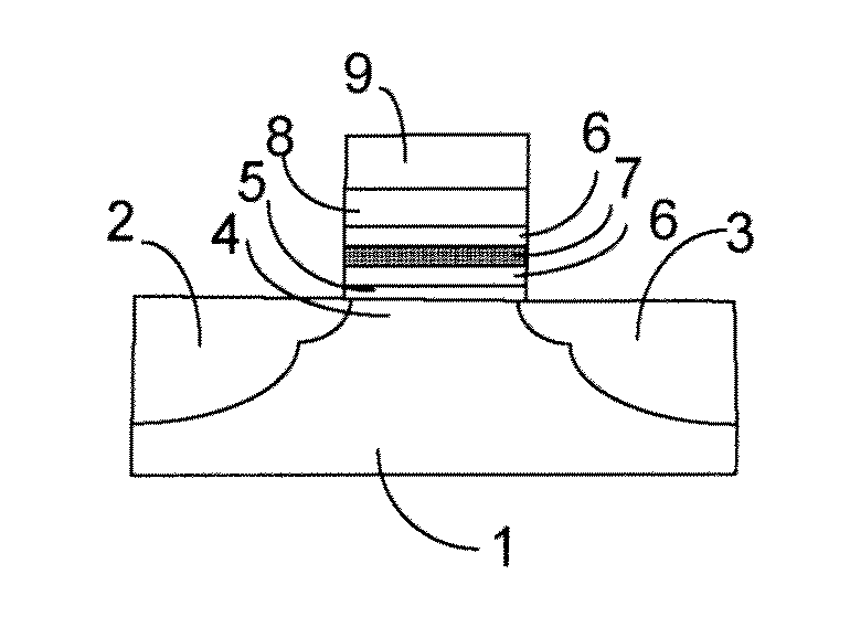
Refer to FIG. 1 for a schematic diagram of a memory structure according to the present invention. As shown in FIG. 1, the non-volatile memory comprises a semiconductor substrate 1, a doped source area 2 and a drain area 3, and a channel area 4 between the source area and drain area, all formed in the semiconductor substrate 1. A first insulation layer 5 is provided on the semiconductor substrate 1. A charge storage layer 6 made of polysilicon is disposed on the first insulation layer 5. An Si1-xGex conductor layer 7 is provided in the charge storage layer 6.
A second insulation layer 8 is provided on the charge storage layer 6. A control gate 9 made of polysilicon or other conductive material is provided on the second insulation layer 8. The second insulation layer 8 is made of silicon oxide, silicon nitride, silicon nitrogen oxide, other dielectric layer of high dielectric constant, or any combinations thereof, such as the dielectric structure of Oxide-Nitride-Oxide (ONO) or the die...
second embodiment
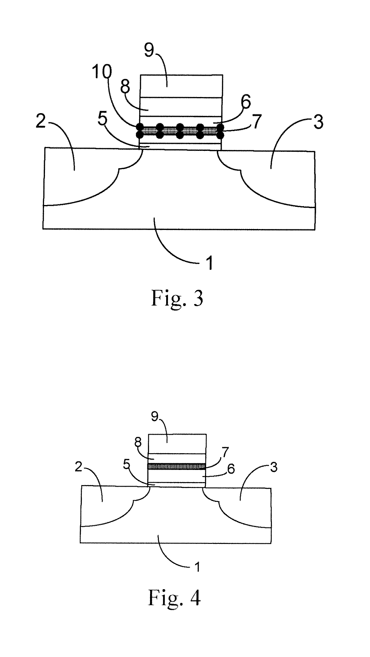
Refer to FIG. 4 for a schematic diagram of a memory structure according to the present invention. As shown in FIG. 4, the non-volatile memory comprises a semiconductor substrate 1, a doped source area 2 and a drain area 3, and a channel area 4 between the source area and the drain area, all formed in the semiconductor substrate 1. A first insulation layer 5 is provided on the semiconductor substrate 1 A charge storage layer 6 made of polysilicon is disposed on the first insulation layer 5. An Si1-xGex conductor layer 7 is provided on the charge storage layer 6 and the range of x value for Si1-xGex conductor layer 7 is 0-1.
A second insulation layer 8 is provided on the Si1-xGex conductor layer 7 and a control gate 9 made of polysilicon or other conductive material is provided on the second insulation layer 8. The second insulation layer 8 is made of silicon oxide, silicon nitride, silicon nitrogen oxide, other dielectric layer of high dielectric constant, or any combinations thereof,...
third embodiment
Refer to FIG. 5 for a schematic diagram of a memory structure according to the present invention. As shown in FIG. 5, anon-volatile memory comprises a semiconductor substrate 1, a doped source area 2 and a drain area 3, and a channel area 4 between the source area 2 and the drain area 3, all formed in the semiconductor substrate 1. A first insulation layer 5 is provided on the semiconductor substrate 1 and a charge storage layer 6 made of polysilicon is disposed on the first insulation layer 5. An Si1-xGex conductor layer 7 is provided in the charge storage layer 6, and the range of x value for the Si1-xGex conductor layer 7 is 0-1.
On a side of the charge storage layer 6 a control gate 9 made of polysilicon or other conductive materials is provided. The second insulation layer 8 is used to separate the charge storage layer 6 and the control gate 9. The second insulation layer 8 is made of silicon oxide, silicon nitride, silicon nitrogen oxide, other dielectric layer of high dielectr...
PUM
 Abstract
Description
Claims
Application Information