Graphene/(multilayer) boron nitride heteroepitaxy for electronic device applications

a boron nitride and heteroepitaxy technology, applied in the direction of vacuum evaporation coating, semiconductor/solid-state device details, transportation and packaging, etc., can solve the problem of inability to grow or integrate, the transfer of graphene sheets grown by this second method is not practical, and the inability to achieve large-scale production of electronic devices with consistent results

Inactive Publication Date: 2011-02-24
UNIVERSITY OF NORTH TEXAS
View PDF9 Cites 45 Cited by
  • Summary
  • Abstract
  • Description
  • Claims
  • Application Information

AI Technical Summary

Benefits of technology

[0012]In accordance with an embodiment of the present invention, large

Problems solved by technology

These methods tend to be impractical for large-scale production of electronic devices with consistent electronic properties, including graphene-substrate contact characteristics.
The transfer of graphene sheets grown by this second method is not practical.
In addition, the growth process occurs at temperatures greater than 1500 K and does not allow for growth or integration with any device materials other than SiC—a materi

Method used


Image

  • Graphene/(multilayer) boron nitride heteroepitaxy for electronic device applications
  • Graphene/(multilayer) boron nitride heteroepitaxy for electronic device applications
  • Graphene/(multilayer) boron nitride heteroepitaxy for electronic device applications

Examples


Embodiment Construction

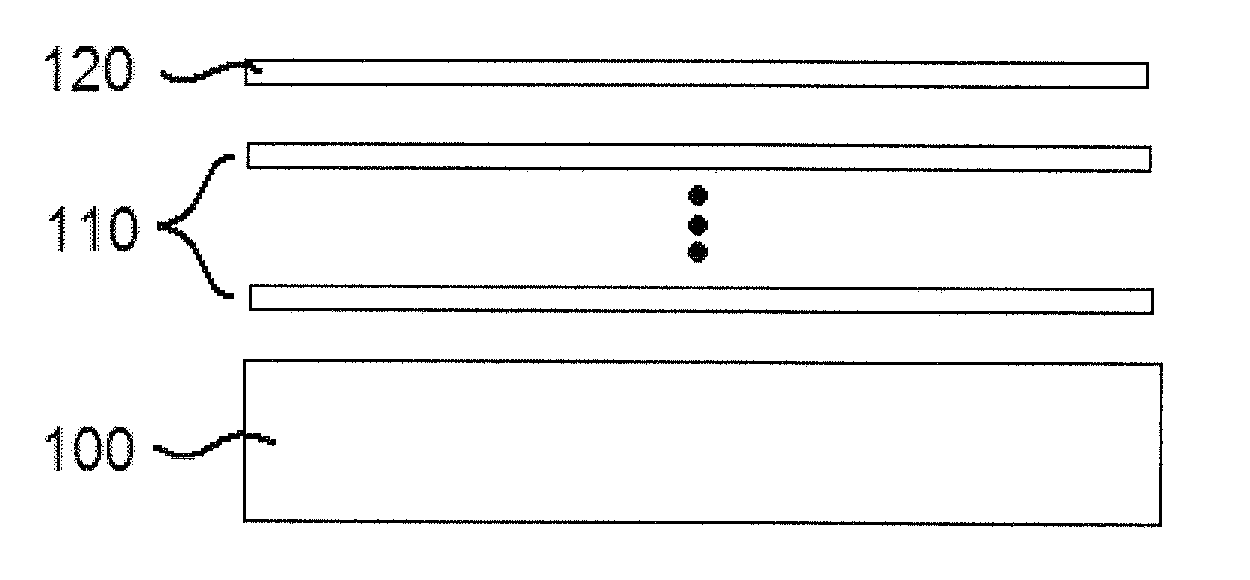
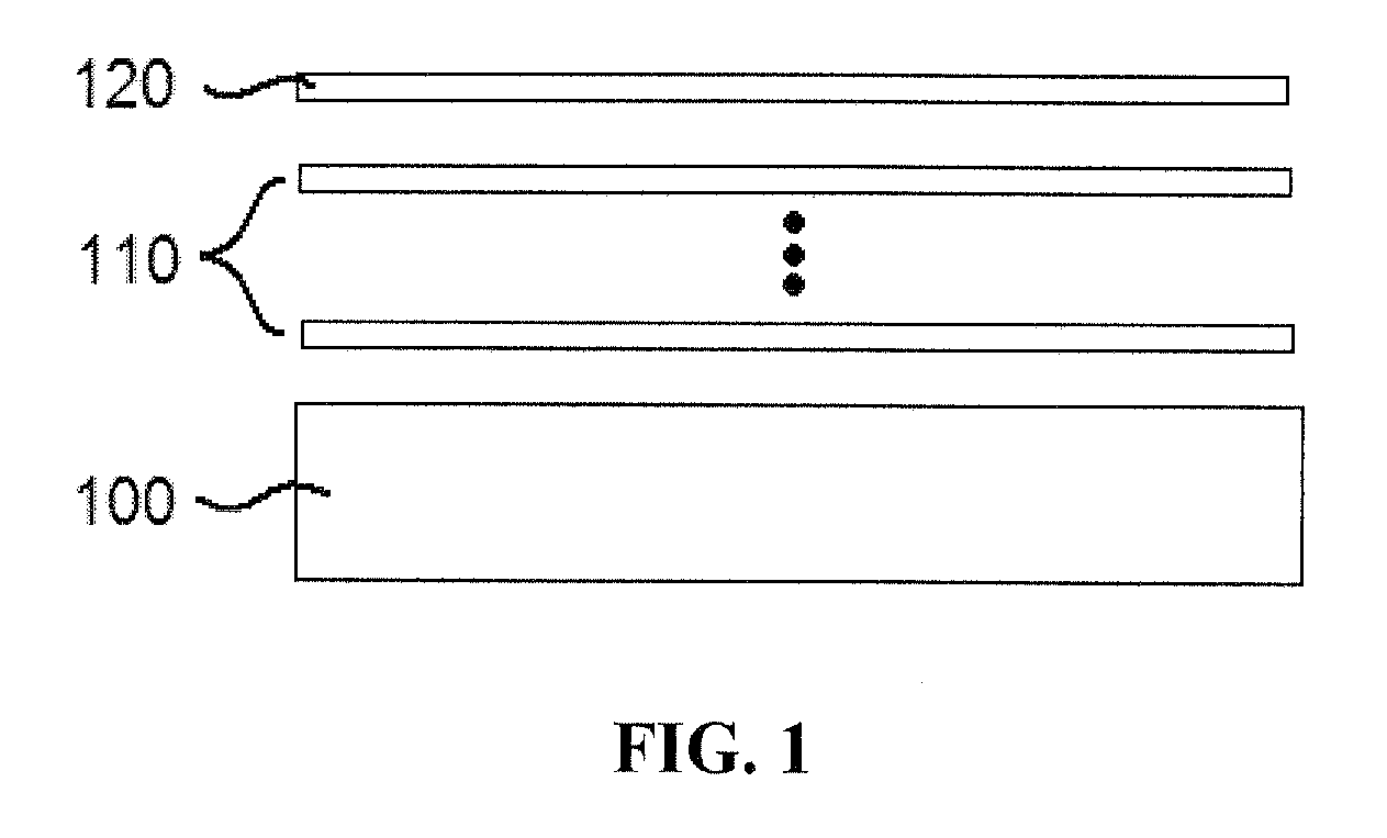
[0016]Embodiments of the present invention provide a substrate-mediated assembly for graphene structures. According to an embodiment, long-range ordered, multilayer BN(111) films can be formed by atomic layer deposition (ALD) onto a substrate. Because BN(111) films are isostructural and isoelectronic with graphene, thereby providing a chemically inert template, the BN(111) films are useful for subsequently ordering carbon atoms into a graphene sheet. In particular, the (111) in-plane lattice constant of BN is 2.50 Å, which is a close lattice match to graphene (2.46 Å). Accordingly, in a further embodiment of the present invention, the subject BN(111) films can then be used to order carbon atoms into a graphene sheet during a carbon deposition process.

[0017]Current CMOS devices are approaching certain physical limits due to continual reduction in the sizes of device features, such as the gate oxide thickness and interconnect line width, the wave nature of electrons manifested on atom...


PUM

PropertyMeasurementUnit
Temperatureaaaaaaaaaa
Pressureaaaaaaaaaa
Massaaaaaaaaaa

Abstract

Disclosed is a substrate-mediated assembly for graphene structures. According to an embodiment, long-range ordered, multilayer BN(111) films can be formed by atomic layer deposition (ALD) onto a substrate. The subject BN(111) films can then be used to order carbon atoms into a graphene sheet during a carbon deposition process.

Description

[0001]The subject invention was made, in part, with government support from the Office of Naval Research contract No. N00014-08-1-1107 through a subcontract from the Texas State University at San Marcos. The government has certain rights in the invention.BACKGROUND OF THE INVENTION[0002]Graphene is a single atomic layer of graphite, and currently holds interest for many electronic and spintronic device applications due to graphene's electronic properties, including high mobility, high saturation velocity, stable crystal structure, and ultrathin layer thickness. To be utilized in electronic and spintronic device applications, graphene must rest on an electronically semiconducting or insulating substrate.[0003]Current methods of producing graphene involve either growing graphene on a transition metal substrate and then transferring a single graphene sheet onto an insulating substrate, or growing graphene by thermal evaporation of silicon from bulk SiC(0001) substrates.[0004]In the fir...

Claims


Application Information

Patent Timeline
IPC IPC(8): B32B9/00B05D5/12C23C14/34B32B15/04
CPCB82Y30/00B82Y40/00C01B31/0453C23C16/26C23C16/342H01L21/02112Y10T428/24355H01L21/823871H01L23/53276B32B9/041Y10T428/24967Y10T428/261H01L21/0228H01L2924/0002C01B32/186H10N70/00H01L2924/00
Inventor KELBER, JEFFRY
Owner UNIVERSITY OF NORTH TEXAS
Why Eureka
Try Eureka