Insulating film, method of manufacturing the same, and semiconductor device

a technology of insulating film and semiconductor, which is applied in the direction of inorganic insulators, thin/thick film capacitors, fixed capacitors, etc., can solve the problems of increasing leakage current, limiting the thickness of insulating film, and a certain level of leakage current, so as to achieve small leakage current, easy formation, and high dielectric constant

Inactive Publication Date: 2011-03-03
ELPIDA MEMORY INC
View PDF20 Cites 310 Cited by
  • Summary
  • Abstract
  • Description
  • Claims
  • Application Information

AI Technical Summary

Benefits of technology

[0039]An exemplary aspect of the invention can provide an insulating film which has a high dielectric constant and has small leakage current when it is sandwiched between electrodes. When a memory cell of a DRAM device is configured using the capacitor element in which an insulating film of an exemplary aspect of the invention is sandwiched between electrodes, the DRAM device can be easily formed which has an excellent data retention characteristic even when the DRAM device is made smaller and the size of the memory cell is reduced. Moreover, a nonvolatile memory device having an excellent leakage characteristic can be easily formed using an insulating film of an exemplary aspect of the invention.

Problems solved by technology

However, the crystallized zirconium oxide had a problem of increase of leakage current as compared to the amorphous zirconium oxide.
However, in case of the insulating film using the uncrystallized zirconium oxide, if the film thickness is made too much smaller, the leakage current exceeds a certain level, so that there exists a limitation in making the insulating film thinner.
Thus, it is impossible to further increase the electrostatic capacitance of the insulating film sandwiched between electrodes.
That is, it is difficult to form an element such as a capacitor, having a reduced occupied area that is provided corresponding to the miniaturization thereof, using an uncrystallized zirconium oxide, because the uncrystallized zirconium oxide has a small dielectric constant.

Method used


Image

  • Insulating film, method of manufacturing the same, and semiconductor device
  • Insulating film, method of manufacturing the same, and semiconductor device
  • Insulating film, method of manufacturing the same, and semiconductor device

Examples


first embodiment

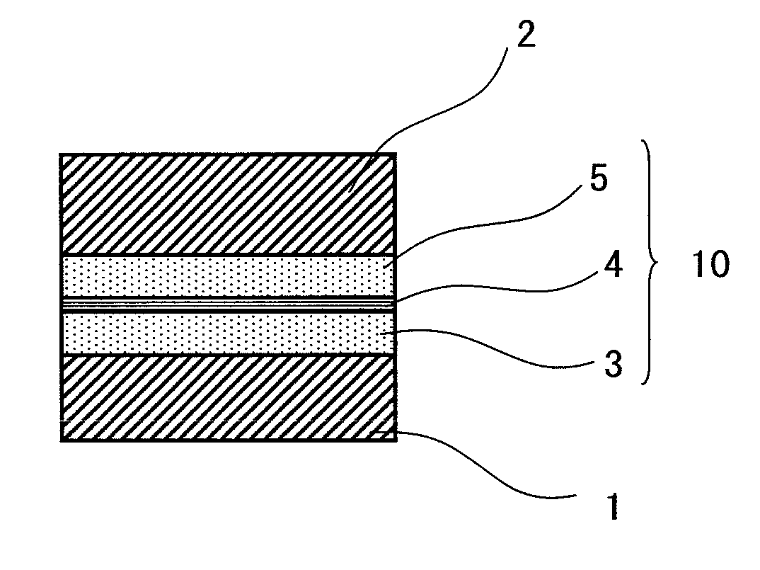
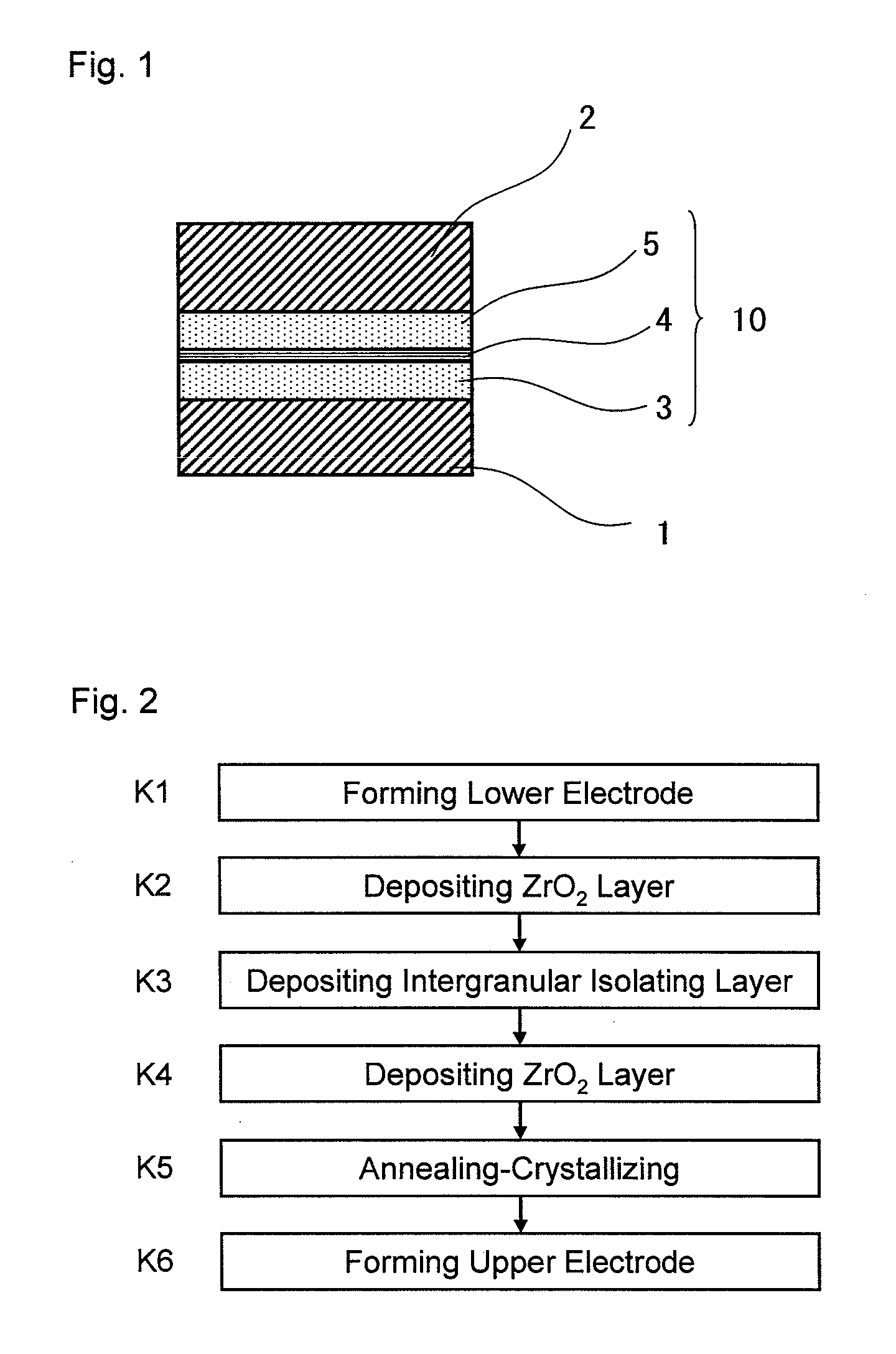
[0054]FIG. 1 is a schematic cross-sectional view showing a structure of a capacitor element having an insulating film according to a first embodiment.

[0055]The capacitor element is formed such that a multi-layered insulating film 10 is sandwiched between a lower electrode 1 and an upper electrode 2 that are composed of a conductive material such as a titanium nitride (TiN). The insulating film 10 is configured by forming an intergranular isolating layer 4 on a crystallized zirconium oxide (ZrO2) layer 3 and by further forming thereon a crystallized zirconium oxide layer 5. The thicknesses of zirconium oxide layers 3 and 5 may be equal to or different from each other.

[0056]The intergranular isolating layer 4 is an insulating layer that has a specific dielectric constant higher than that of a crystallized zirconium oxide layer, and has a function of separating grain boundaries of the zirconium oxide, thereby restricting leakage current from flowing between the lower electrode 1 and th...

modified embodiment of first embodiment

[0114]FIG. 7 is a schematic cross-sectional view showing a structure of a capacitor element having an insulating film according to an exemplary embodiment. An insulating film of an exemplary embodiment may be provided with two or more intergranular isolating layers.

[0115]In FIG. 7, a multi-layered insulating film 10 is arranged between a lower electrode 1 and an upper electrode 2 so as to form a capacitor. The insulating film 10 is configured such that two intergranular isolating layers 4 and 6 are sandwiched among three crystallized zirconium oxide layers 3, 5 and 7.

[0116]The insulating film 10 can be formed by sequentially depositing respective layers constituting the insulating film using an ALD method. The intergranular isolating layer may be a TiAlO layer. In this case, it is preferable to set a content of aluminum oxide component in each of the TiAlO layers in a range of from 5 to 15 atomic %. Meanwhile, when the intergranular isolating layer consists of two or more layers, th...

second embodiment

[0117]In the followings, it will be described a case where an exemplary embodiment is applied to a capacitive insulating film of a capacitor element constituting a memory cell of a DRAM device, which is a specific example to which an insulating film of an exemplary embodiment is applied.

[0118]FIG. 8 is a schematic diagram showing a planar layout of a memory cell part of a DRAM device to which an insulating film of an exemplary embodiment is applied. The right side of FIG. 8 is shown as a perspective sectional view based on a surface that cuts a gate electrode 105 and a side wall 105b that will be a word wiring (W), as described below. FIG. 9 is schematic cross-sectional view taken along line A-A′ shown in FIG. 8. In addition, for simplification, a capacitor element is not shown in FIG. 8, but is only shown in FIG. 9. Meanwhile, the drawings are provided only to explain a structure of a semiconductor device and it should be understood that dimensions or sizes of each part shown may b...


PUM

PropertyMeasurementUnit
thicknessaaaaaaaaaa
thicknessaaaaaaaaaa
dielectric constantaaaaaaaaaa

Abstract

An exemplary aspect of the invention provides an insulating film which has a high dielectric constant and has small leakage current even when it is sandwiched between electrodes. The insulating film comprises two zirconium oxide layers in crystallized state; and an intergranular isolating layer composed of an amorphous material having a dielectric constant higher than that of zirconium oxide in crystallized state; wherein the intergranular isolating layer is sandwiched between the two zirconium oxide layers. The insulating film is properly used as a capacitive insulating film in a semiconductor device comprising a memory cell including a capacitor element having the capacitive insulating film between an upper electrode and a lower electrode, or as an intergate insulating film in a semiconductor device comprising a nonvolatile memory device having the intergate insulating film between a control gate electrode and a floating gate electrode.

Description

[0001]This application is based upon and claims the benefit of priority from Japanese patent application no. 2009-201448, filed on Sep. 1, 2009, the disclosure of which is incorporated herein in its entirety by reference.BACKGROUND OF THE INVENTION[0002]1. Field of the Invention[0003]An exemplary aspect of the invention relates to an insulating film, a method of manufacturing the same, a semiconductor device, and a data processing system.[0004]2. Description of the Related Art[0005]With high integration of the semiconductor device, demand for an insulating film (a dielectric film) with a high dielectric constant and low leakage current is increasing. For example, capacitor-mounted devices such as DRAM devices require an insulating film with a high dielectric constant and low leakage current as means that do not reduce as much electrostatic capacitance as possible even when the size of a memory cell becomes smaller owing to miniaturization.[0006]Insulating films that satisfy the dema...

Claims


Application Information

Patent Timeline
Patent Type & Authority Applications(United States)
IPC IPC(8): H01B3/00
CPCH01B3/12H01L21/02178H01L21/02186H01L21/02189H01L21/02194H01L21/022H01L29/7881H01L21/28273H01L27/10852H01L28/40H01L28/91H01L29/513H01L29/517H01L21/0228H01L29/40114H01G4/1236H01G4/33H10B12/033
Inventor FUJIWARA, NAONORI
Owner ELPIDA MEMORY INC
Why Eureka
Try Eureka