

Organic electroluminescent device
a technology of electroluminescent devices and electroluminescent devices, which is applied in the direction of luminescent compositions, thermoelectric devices, organic chemistry, etc., can solve the problems of reducing the efficiency, reducing the luminous efficiency, and lowering the efficiency of used materials, so as to achieve efficient injection or transportation of holes, effectively reveal the role of injection or transportation, and improve the effect of hole injection performan
- Summary
- Abstract
- Description
- Claims
- Application Information
AI Technical Summary
Benefits of technology
Problems solved by technology
Method used
Image

Examples
example 1a
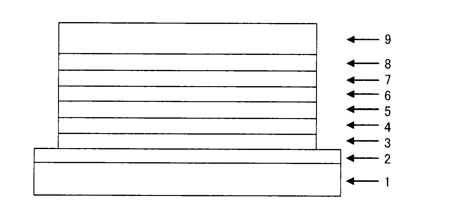
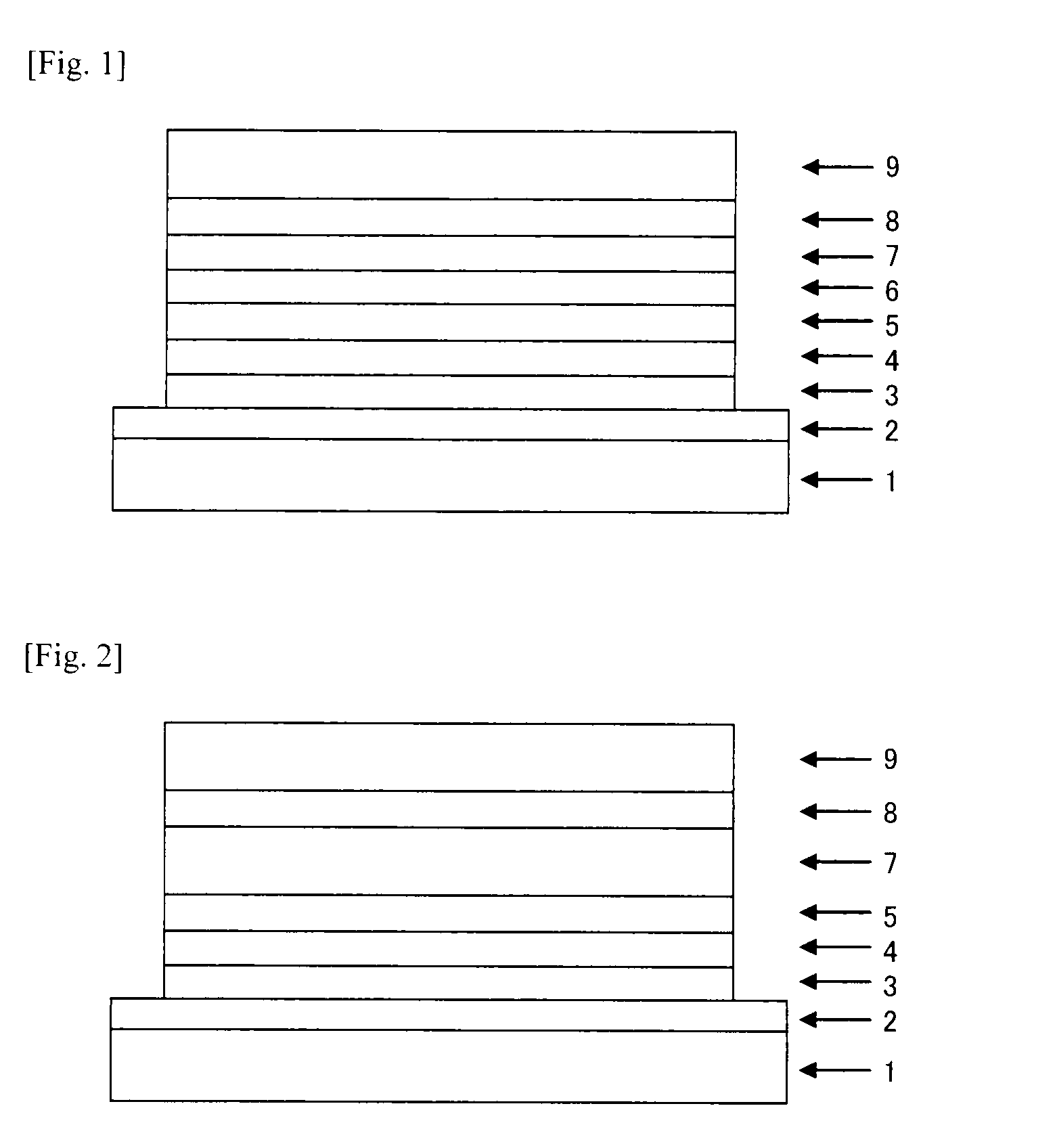
[0087]An organic EL device was prepared by depositing a hole-injecting layer 3, a hole-transporting layer 4, an emitting layer 5, an electron-transporting layer 7, an electron-injecting layer 8 and a cathode (aluminum electrode) 9 in this order on a glass substrate 1 on which an ITO electrode had been formed as a transparent anode 2 in advance, as shown in FIG. 2.
[0088]First of all, after the glass substrate 1 on which ITO having a film thickness of 150 nm had been formed was ultrasonically washed in isopropyl alcohol for 20 minutes, it was washed by boiling on a hot plate heated at 150° C. for 20 minutes. Thereafter, this ITO-provided glass substrate was mounted in a vacuum deposition machine and subjected to an oxygen plasma treatment for 5 minutes, following by evacuating to 0.001 Pa or lower.
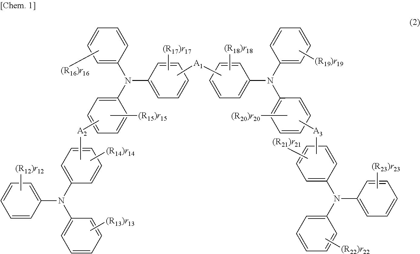
[0089]Subsequently, Compound 2-1 of the following structural formula was formed in a film thickness of 20 nm as the hole-injecting layer 3 so as to cover the transparent electrode 2. On this...
example 2a
[0091]An organic EL device was prepared in the same manner as in Example 1A except that Compound 3-1 was formed in a film thickness of 100 nm as the hole-transporting layer 4.
[0092]The thus prepared organic EL device was measured for characteristics upon being applied with a direct current voltage at ordinary temperature in the air. As a result, a driving voltage at the time of flowing of a current with a current density of 10 mA / cm2 was found to be 5.45 V.
example 3a
[0093]An organic EL device was prepared in the same manner as in Example 1A except that Compound 3-1 was formed in a film thickness of 150 nm as the hole-transporting layer 4.
[0094]The thus prepared organic EL device was measured for characteristics upon being applied with a direct current voltage at ordinary temperature in the air. As a result, a driving voltage at the time of flowing of a current with a current density of 10 mA / cm2 was found to be 6.65 V.
PUM
 Abstract
Description
Claims
Application Information