Charge trapping memory cell having bandgap engineered tunneling structure with oxynitride isolation layer

a charge-trapping memory cell and tunneling structure technology, applied in the field of flash memory technology, can solve the problems of limiting the ability to increase the density of flash memory, affecting the speed of erase, and affecting the endurance and charge retention characteristics of memory cells relative to traditional floating gate technology, so as to achieve the effect of increasing the speed of erase in the hole tunneling

Active Publication Date: 2011-03-31
MACRONIX INT CO LTD
View PDF9 Cites 15 Cited by
  • Summary
  • Abstract
  • Description
  • Claims
  • Application Information

AI Technical Summary

Benefits of technology

[0007]The performance achieved using BE-SONOS devices characterized by having a dielectric tunneling structure including a tunneling layer, a band offset layer and an isolation layer as described above, is further improved by engineering the isolation layer, replacin

Problems solved by technology

As the density increases in memory devices, and the floating gate memory cells get closer and closer together, interference between the charge stored in adjacent floating gates becomes a problem.
This interference limits the ability to increase the density of flash memory based on floating gate memory cells.
However at that thickness, the endurance and charge retention cha

Method used


Image

  • Charge trapping memory cell having bandgap engineered tunneling structure with oxynitride isolation layer
  • Charge trapping memory cell having bandgap engineered tunneling structure with oxynitride isolation layer
  • Charge trapping memory cell having bandgap engineered tunneling structure with oxynitride isolation layer

Examples


Embodiment Construction

with various concentrations of nitrogen.

[0035]FIG. 20 plots the results of testing charge trapping efficiency by applying ISPP programming operations to test structures having SiON charge trapping layers with various concentrations of nitrogen.

[0036]FIG. 21 is a schematic diagram of a NAND-type memory array employing memory cells according to the present invention.

[0037]FIG. 22 is a simplified cross-sectional view of memory cells according to the present invention in a NAND configuration, taken perpendicular to word lines.

[0038]FIG. 23 is a simplified cross-sectional view of memory cells according to the present invention in a NAND configuration, taken through a word line.

[0039]FIG. 24 is a block diagram of an integrated circuit memory employing memory cells and bias circuitry according to embodiments of the present invention.

DETAILED DESCRIPTION

[0040]A detailed description of embodiments of the present invention is provided with reference to the FIGS. 1-24.

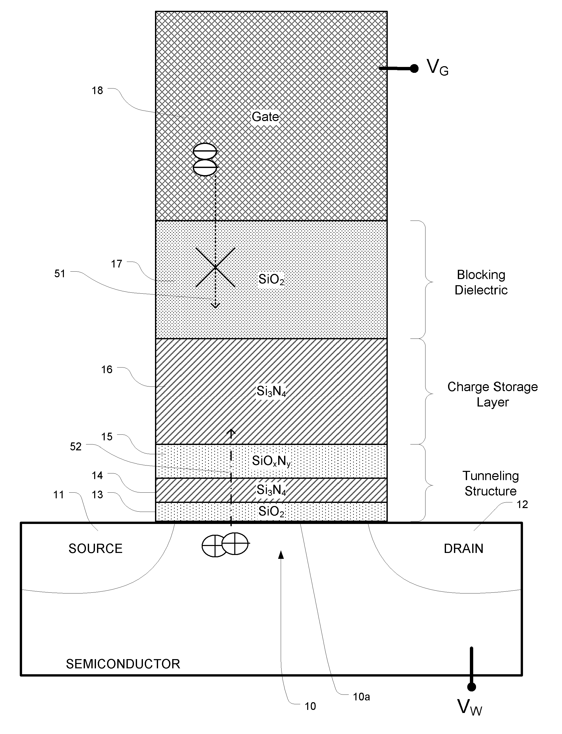
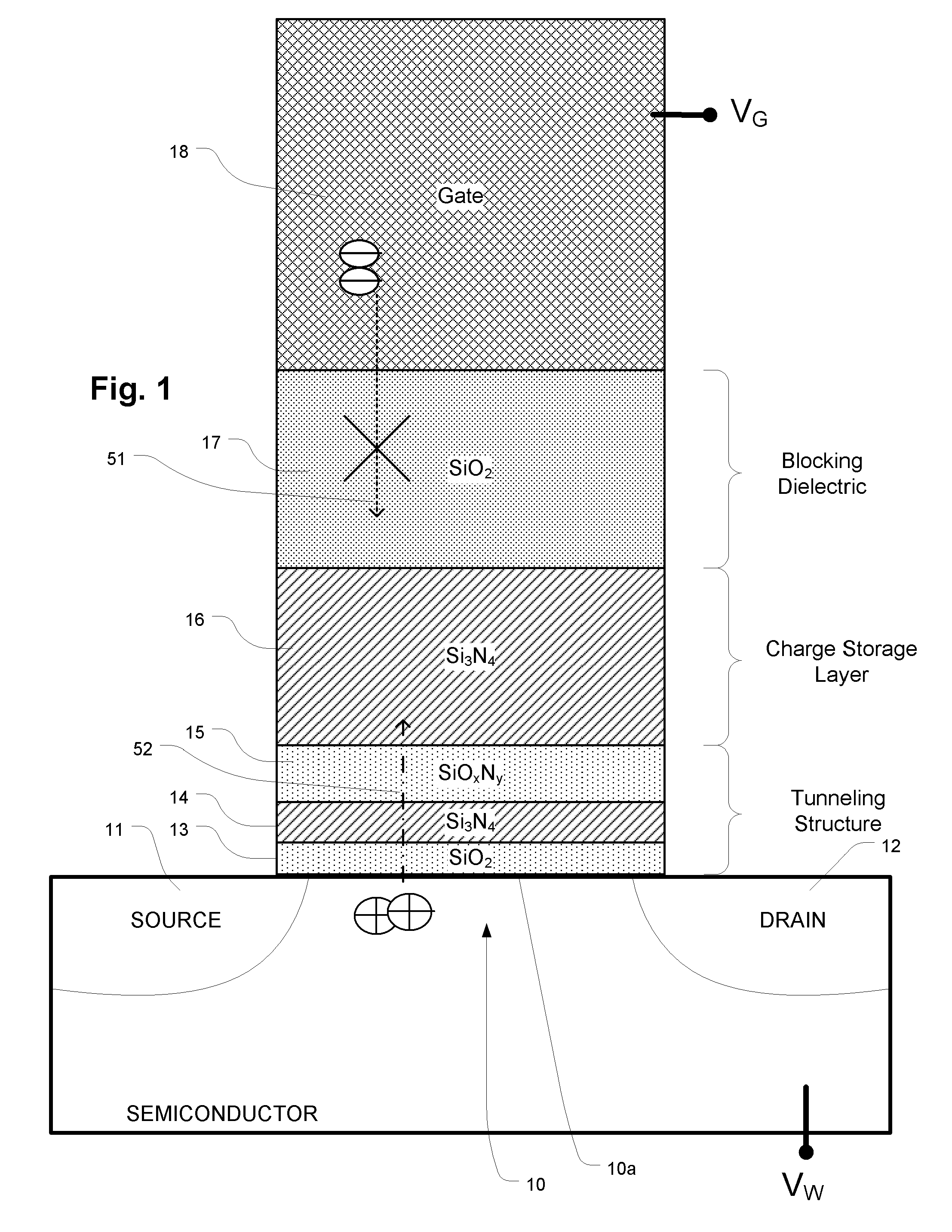
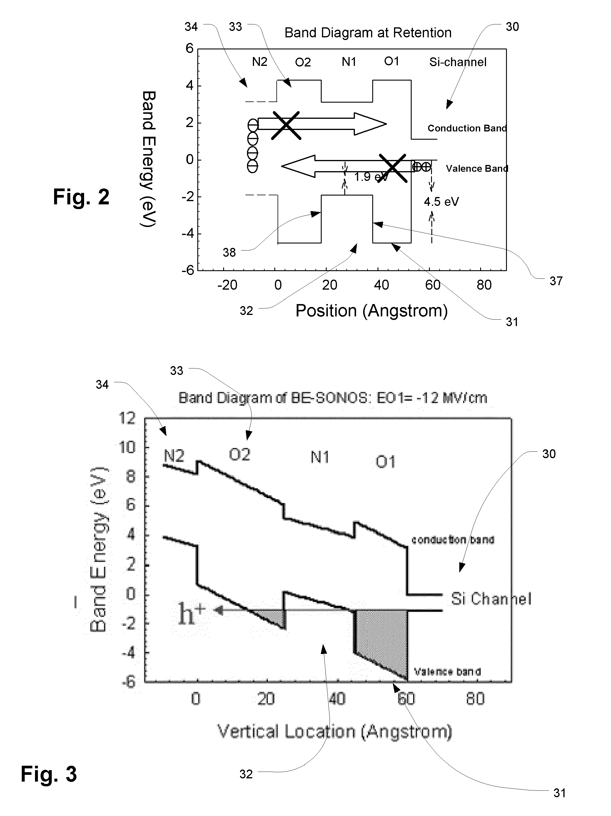
[0041]FIG. 1 is a simplif...


PUM


Abstract

A band gap engineered, charge trapping memory cell includes a charge storage structure including a trapping layer. a blocking layer, and a dielectric tunneling structure including a thin tunneling layer, a thin bandgap offset layer and a thin isolation layer comprising silicon oxynitride. The memory cell is manufactured using low thermal budget processes.

Description

FIELD OF THE INVENTION[0001]The present invention relates to flash memory technology, and more particularly to scalable charge trapping memory technology adaptable for high speed erase and program operations.DESCRIPTION OF RELATED ART[0002]Flash memory is a class of non-volatile integrated circuit memory technology. Traditional flash memory employs floating gate memory cells. As the density increases in memory devices, and the floating gate memory cells get closer and closer together, interference between the charge stored in adjacent floating gates becomes a problem. This interference limits the ability to increase the density of flash memory based on floating gate memory cells. Another type of memory cell used for flash memory can be referred to as a charge trapping flash memory cell, which uses a dielectric charge trapping layer in place of the floating gate. Charge trapping memory cells use dielectric charge trapping material that causes much less cell-to-cell interference than ...

Claims


Application Information

Patent Timeline
IPC IPC(8): G11C16/04H01L29/792H01L21/336
CPCH01L21/28282H01L27/11568H01L29/792H01L29/513H01L29/518H01L29/4234H01L29/40117H10B43/30
Inventor LIAO, JENG-HWASHIEH, JUNG-YUYANG, LING-WUU
Owner MACRONIX INT CO LTD
Why Eureka
Try Eureka