

P-type NiO conducting film for organic solar cell, a method for preparation of NiO conducting film, and an organic solar cell with enhanced light-to-electric energy conversion using the same
a solar cell and conducting film technology, applied in the direction of organic semiconductor devices, solid-state devices, synthetic resin layered products, etc., can solve the problems of low-melting substrate method that is difficult to apply, limited corrosion of ald reactors, and high production costs, and achieves enhanced power conversion efficiency, easy preparation, and enhanced power conversion efficiency
- Summary
- Abstract
- Description
- Claims
- Application Information
AI Technical Summary
Benefits of technology
Problems solved by technology
Method used
Image

Examples
embodiment 1
Preparation of a P-Type NiO Conducting Film for an Organic Solar Cell
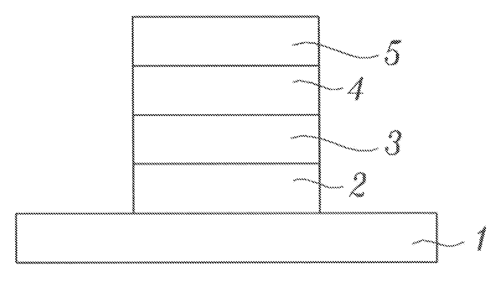
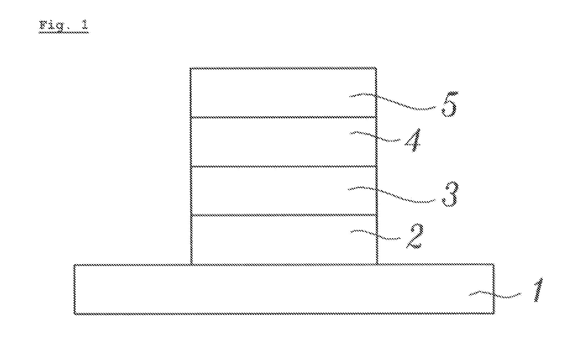
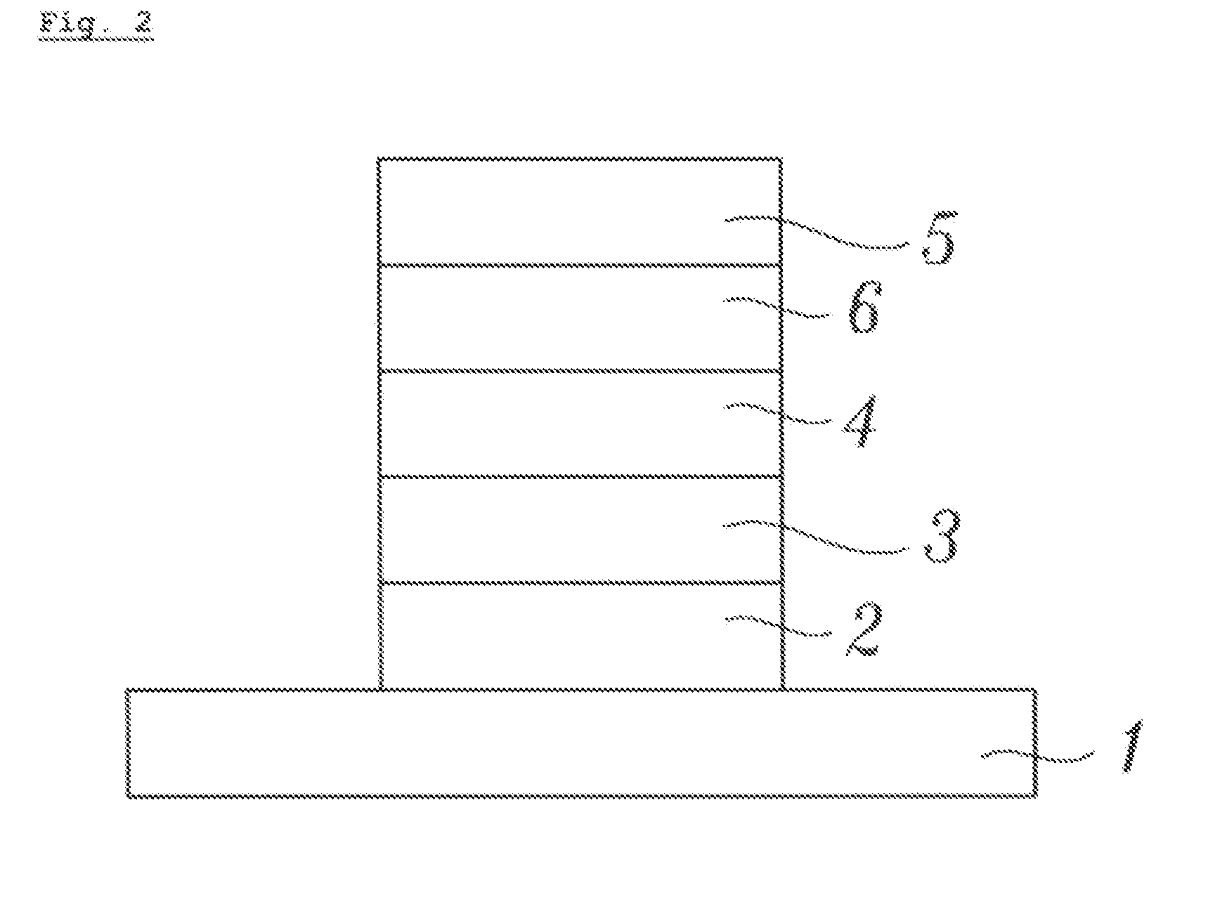
[0047]Substrate was coated with indium tin oxide (ITO) and ultra-sonic washed with the addition of acetone for 10 minutes and then washed with ozonator for 10 minutes. On the surface of the ITO coating, a 50 nm-thick NiO conducting film was deposited by vacuum sputtering under processing pressure of 5 mTorr for 60 seconds in which nickel or nickel oxide was used as a target material, 50 sccm of a mixed gas of argon and oxygen was supplied, and RF power as 100 W was applied.
embodiment 2
Preparation 1 of an Organic Solar Cell
[0048]Substrate was coated with indium tin oxide (ITO) and ultra-sonic washed with the addition of acetone for 10 minutes and then washed with ozonator for 10 minutes. On the surface of the ITO coating, a 3 nm-thick NiO conducting film was deposited by vacuum sputtering under 5 mTorr for 60 seconds in which nickel or nickel oxide was used as a target material, and 50 sccm of oxygen was supplied. A photoactive layer 200 nm in thickness was deposited on the NiO conducting film, by mixing 20 mg of P3HT (poly(3-hexylthiophene)) and 20 mg of PCBM, as photoactive substances, with 1 ml of dichlorobenzene solution to prepare a photoactive layer solution, and spin-coating the solution at 600 rpm. The thin film was then thermally treated at 150° C. for 20 minutes using glove box, and a LiF / Al cathode (LiF / AI) was prepared in a manner of depositing the LiF to a thickness of 1.0˜1.5 nm using thermal evaporator for 0.1 A / sec, and aluminum was deposited to a ...
embodiment 3
Preparation 2 of an Organic Solar Cell
[0049]Except for the fact that the NiO conducting film 5 nm in thickness was deposited by the vacuum sputtering for 100 seconds, the rest of the process of preparing an organic solar cell is the same as that of Embodiment 2.
PUM
| Property | Measurement | Unit |
|---|---|---|
| thickness | aaaaa | aaaaa |
| thickness | aaaaa | aaaaa |
| HOMO Level | aaaaa | aaaaa |
Abstract
Description
Claims
Application Information