

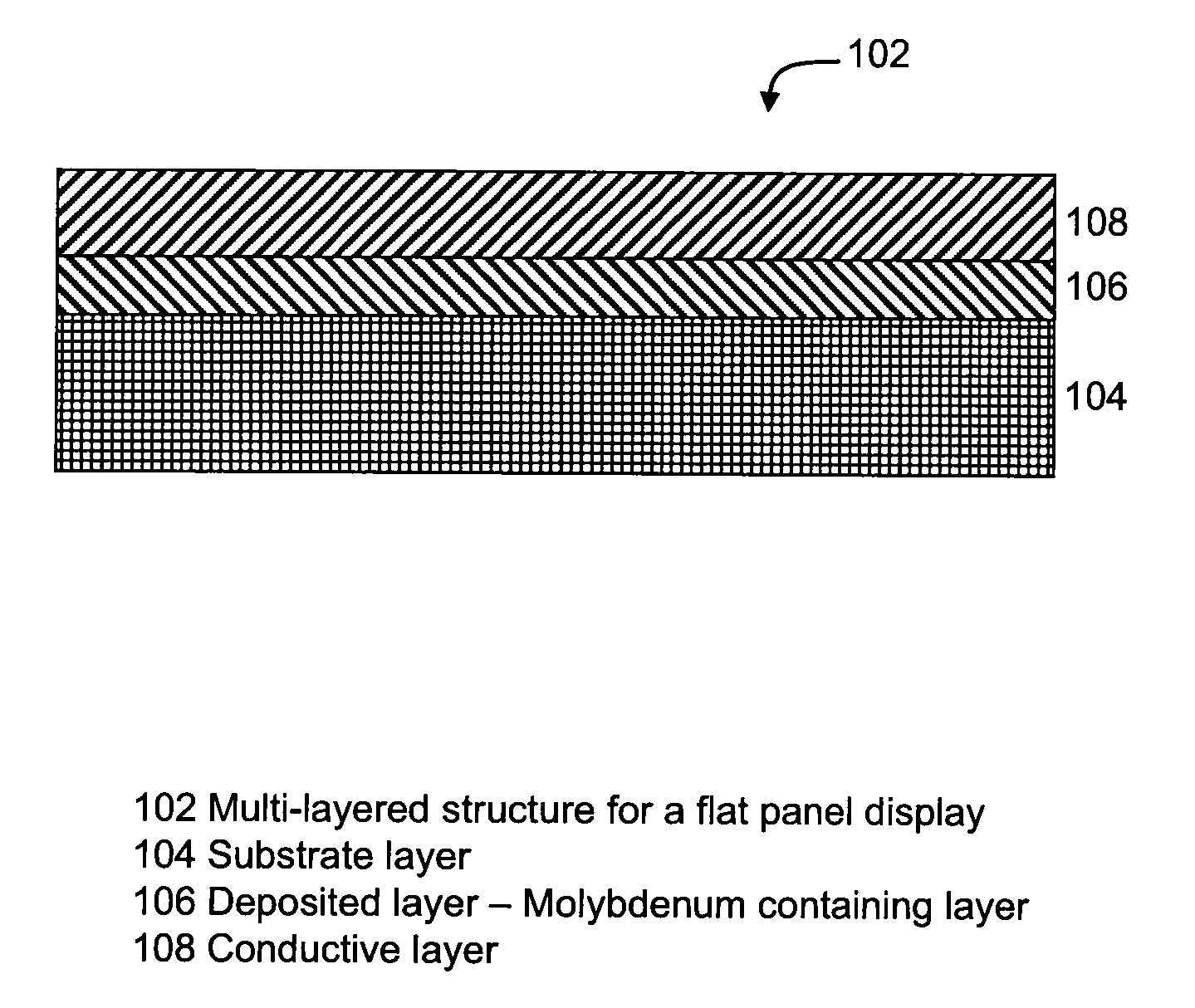
Molybdenum containing targets
a technology of molybdenum and targets, applied in the field of sputter targets, can solve problems such as significant property changes, and achieve the effects of low electrical resistivity, good barrier properties, and efficient production of large sputter targets
- Summary
- Abstract
- Description
- Claims
- Application Information
AI Technical Summary
Benefits of technology
Problems solved by technology
Method used
Image

Examples
examples 1-10
Molybdenum Titanium / Tantalum
[0109]Example 1 illustrates a sputter target including molybdenum, titanium and tantalum. Examples 2-9 illustrate deposited films prepared from the sputter target of Example 1.
example 1
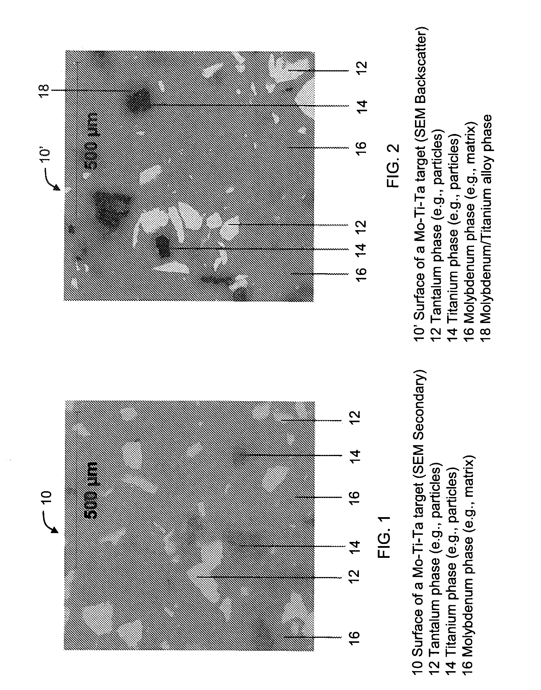
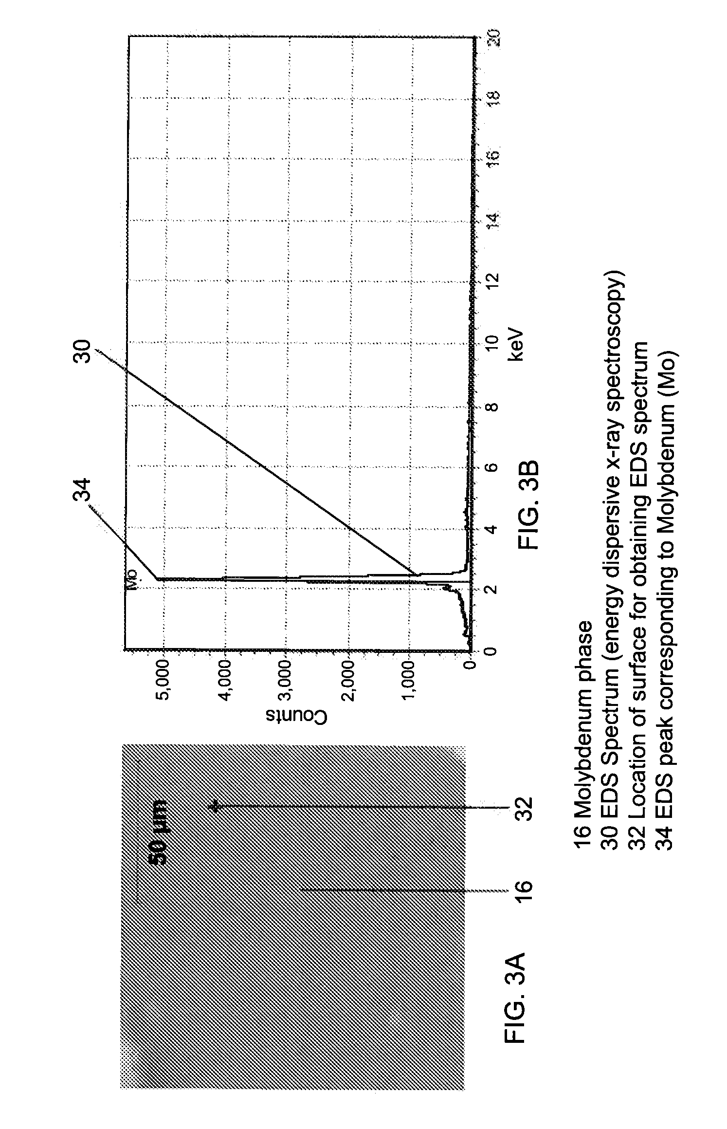
[0110]Example 1 is a sputter target that is prepared by first blending molybdenum powder having a particle size of about 3-4 μm, tantalum powder having a particle size of about 45-90 μm, and titanium powder having a particle size of about 10-45 μm, to form a powder blend having about 80 atomic % molybdenum, about 10 atomic % titanium, and about 10 atomic % tantalum. The blending is done in a V-blender for about 20 minutes to obtain a homogeneous mixture of the three different powders. The resulting powder blend is then consolidated by uniaxially pressing with an applied force of about 340,000 kg into pellets having a diameter of about 95 mm (i.e., a pressure of about 470 MPa) at a temperature of about 23° C. The pressed pellet is then encapsulated in a can made of low carbon steel and hot isostatically pressed at a temperature of about 1325° C. and a pressure of about 100 to about 120 MPa for about 4 hours. Thus prepared, Example 1 has a density which is greater than about 94% of th...
examples 2-9
[0113]Examples 2-9 illustrate a method that includes steps of sputtering a thin film layer using a sputter target as taught herein onto a substrate (e.g., a silicon-containing substrate, or a glass-containing substrate). Sputtering may be performed using a magnetron. In general, sputtering will occur for about 1 to about 240 minutes (preferably about 1 to about 40 minutes), under conditions of vacuum from about 1 to about 100 mTorr pressure (preferably from about 2 to about 20 mTorr pressure), and a spacing between the substrate and the sputter target of about 5 to 300 mm (preferably about 20 to about 150 mm. The resulting structure will have characteristics consistent with examples 2-9 herein.
[0114]Examples 2, 3, 4, 5, 6, 7, 8, and 9 are prepared by placing the sputter target of Example 1 into a magnetron sputter deposition chamber using the conditions described in Table 1. The substrate is either a silicon wafer (100) orientation, or Corning 1737 glass. Prior to deposition, the su...
PUM
| Property | Measurement | Unit |
|---|---|---|
| etch rate | aaaaa | aaaaa |
| thickness | aaaaa | aaaaa |
| length | aaaaa | aaaaa |
Abstract
Description
Claims
Application Information