Field effect transistor, display element, image display device, and system

a field effect transistor and display element technology, applied in static indicating devices, instruments, non-linear optics, etc., can solve the problems of insufficient mobility, a-si tft, and difficulty in meeting all the demands at the same tim

Inactive Publication Date: 2011-06-02
RICOH KK
View PDF18 Cites 47 Cited by
  • Summary
  • Abstract
  • Description
  • Claims
  • Application Information

AI Technical Summary

Benefits of technology

[0040]According to one aspect of the present invention, a field effect transistor includes a gate electrode to which a gate voltage is applied; a source electrode and a drain electrode for obtaining a current in response to the gate voltage; an acti

Problems solved by technology

Therefore, it has been difficult to satisfy all the demands at the same time.
For example, a-Si TFT has disadvantages of insufficient mobility for driving a large screen LCD (Liquid Crystal Display) at a high speed, and a large shift of a threshold voltage in continuous driving.
Although LTPS-TFTs have high mobility, they have a disadvantage in that threshold voltages largely vary due to a process for crystallizing an active layer by annealing using an excimer laser; therefore, a large-sized mother glass for the mass production line cannot be used.
In this case, in view of the heat resistance of the flexible substrate, it has been impossible to use silicon which requires a relatively high temperature process when manufactured.
However, when ZnO, CdO, Cd—In oxide and Cd—Ga oxide are used for an active layer of the TFT, an oxygen vacancy or an interstitial metal atom is easily caused.
Therefore, it has been difficult to achieve the normally-off characterist

Method used


Image

  • Field effect transistor, display element, image display device, and system
  • Field effect transistor, display element, image display device, and system
  • Field effect transistor, display element, image display device, and system

Examples


embodiment 2

[0134]A field effect transistor with a channel length of 5 μm and a channel width of 1.5 mm was obtained by the steps similar to those of Further, by repeating the same steps, four samples of this field effect transistor were manufactured.

[0135]A relationship of a gate voltage VG and a source-drain current IDS of each of these four field effect transistors in the case where a source-drain voltage VDS is 20 V is shown in FIG. 26. The characteristics of the four transistors, which are shown by one solid line and three broken lines with different patterns, clearly vary. For example, there are large differences among the samples in the current value obtained when the transistors are on. Field effect mobility calculated in a saturation region vary from 0.8 to 3.0 cm2 / Vs.

[0136]Contact resistance between the source electrode and the active layer and between the drain electrode and the active layer were about 50 kΩ. On the other hand, resistance of a channel (channel resistance) in the cas...

embodiment 1

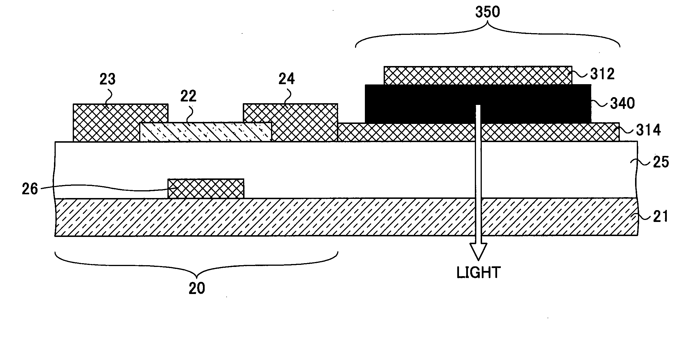
[0145]FIG. 11 shows a positional relationship between the organic EL element 350 of the display element 302 and the field effect transistor 20 described in Here, the organic EL element 350 is arranged beside the field effect transistor 20. The field effect transistor 10 and the capacitor 30 are formed on the same substrate as these elements.

[0146]The display element 302 can be manufactured by using an apparatus and steps (manufacturing process) similar to the conventional ones.

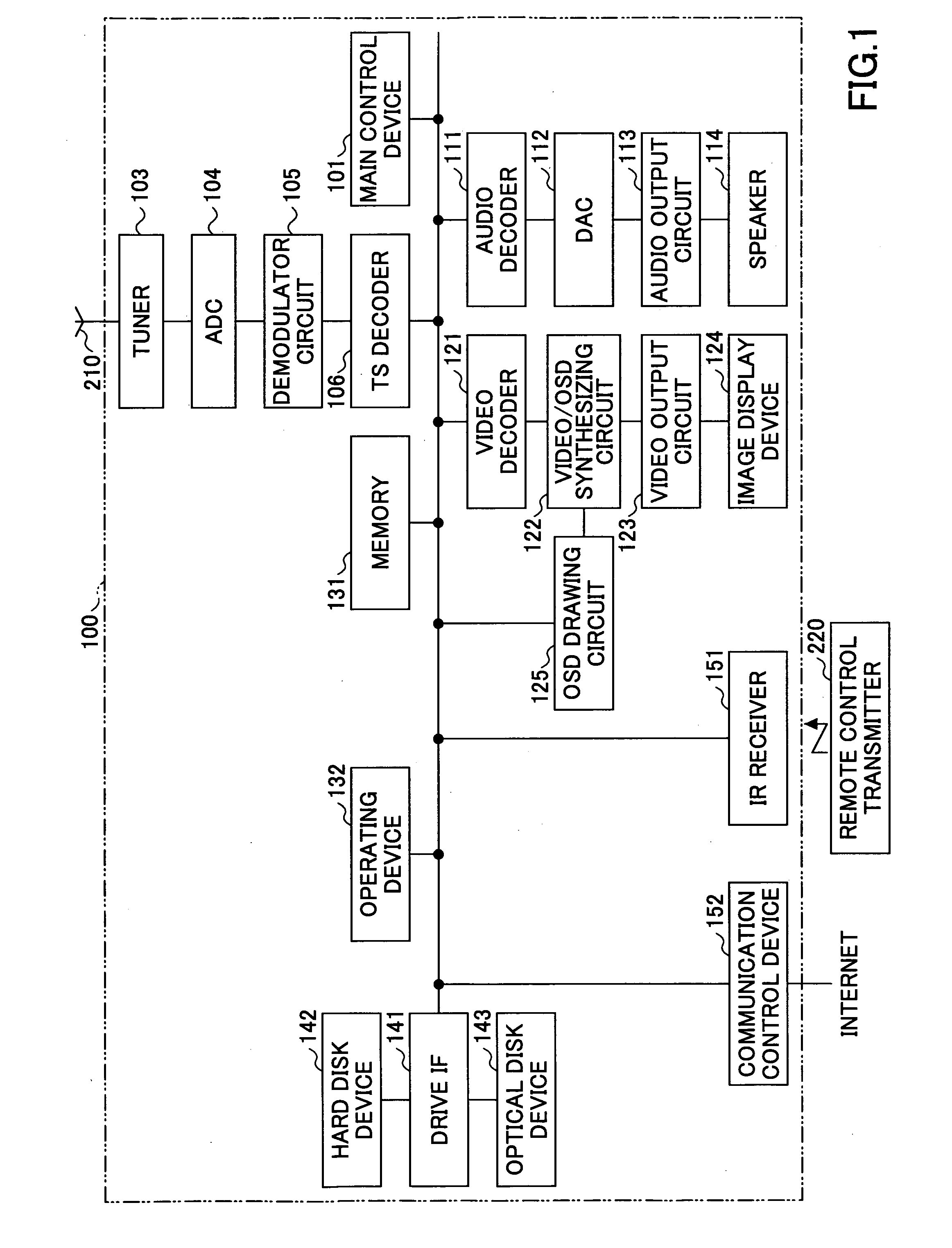
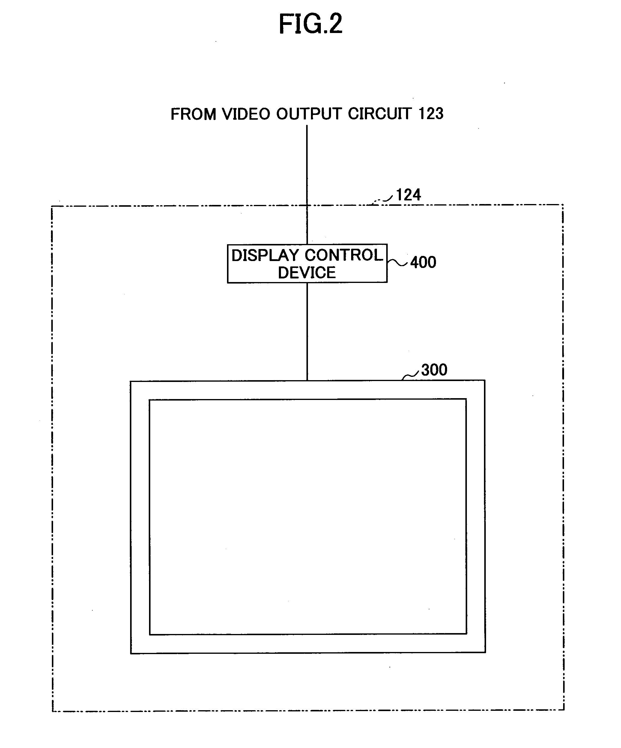
[0147]As shown in an example of FIG. 12, the display control apparatus 400 includes an image data process circuit 402, a scan line driver circuit 404, and a data line driver circuit 406.

[0148]The data processing circuit 402 determines luminance of the plural display elements 302 of the display 310 according to output signals of the video output circuit 123.

[0149]The scan line driver circuit 404 applies a voltage individually to the n scan lines according to instructions of the image data processing circuit 40...


PUM


Abstract

A field effect transistor includes a gate electrode to which a gate voltage is applied; a source electrode and a drain electrode for obtaining a current in response to the gate voltage; an active layer provided adjacent to the source electrode and the drain electrode and formed of an oxide semiconductor including magnesium and indium as major components; and a gate insulating layer provided between the gate electrode and the active layer.

Description

TECHNICAL FIELD[0001]The present invention relates to a field effect transistor, a display element, an image display device, and a system. More particularly, the present invention relates to a field effect transistor having an active layer formed of an oxide semiconductor, a display element and an image display device each including the field effect transistor, and a system having the image display device.BACKGROUND ART[0002]A field effect transistor (FET) is a transistor for controlling a current flowing between a source electrode and a drain electrode by applying a voltage to a gate electrode to provide a gate for the flow of electrons or holes depending on an electric field of a channel.[0003]An FET has been used as a switching element and an amplifying element for its characteristics. Since an FET shows a small gate current and has a flat profile, it can be easily manufactured or integrated compared to a bipolar transistor. Therefore, an FET is now an indispensable element in an...

Claims


Application Information

Patent Timeline
IPC IPC(8): G06F3/038H01L33/28H01L51/52
CPCH01L29/7869H01L27/1225H01L29/78693G02F1/1368H10K59/1213G09G3/3258G09G3/3655G09G2320/043H01L29/04H01L29/24
Inventor UEDA, NAOYUKIABE, YUKIKOKONDO, HIROSHINAKAMURA, YUKISONE, YUJI
Owner RICOH KK
Why Eureka
Try Eureka