Digital power amplifier with i/q combination

a power amplifier and digital technology, applied in the field of electronic circuits, can solve the problems of reducing slowing down the useful life of the amplifier, and not sharing the wonderful benefits of digital scaling with the traditional rf circuit, so as to improve the amplitude resolution of the electronic circui

Inactive Publication Date: 2011-06-02
TECH UNIV DELFT
View PDF2 Cites 45 Cited by
  • Summary
  • Abstract
  • Description
  • Claims
  • Application Information

AI Technical Summary

Benefits of technology

[0031]Embodiments of the invention seeks to provide a solution which fulfils a need for a digital TX architecture that is capable of supporting advanced wideband wireless modulation standards, but which avoids the intrinsic bandwidth expansion issues of the polar topology and the severe noise issues of the conventional digital I / Q architectures.
[0034]The in-phase component and the quadrature component comprise a respective amplitude control word, each of the first and second DRAC's comprising a controllable switch array having an array of AND gates, each AND gate receiving the respective clock signal and one of the bits of the respective ACW, the output of each AND gates being connected to an associated one of a plurality of MOS transistor switches, the outputs of each of the plurality of MOS transistors being connected to a summation node. Such a controllable switch array may be easily implemented in e.g. MOS techniques. In accordance with embodiments, the switch arrays of the first and second DRAC's are implemented in the electronic circuit with an interleaved lay-out. This improves the ease of manufacturing, and also enhances the regularity of the DRAC's so formed.
[0035]In accordance with embodiments, each of the first and second DRAC includes an output impedance connected in series between the output of each MOS transistor and the summation node. This allows to increase the resolution and dynamic range of the RF envelope control (when the impedance accuracy and range are better than those of the transistor switches).
[0036]In accordance with embodiments, the first DRAC and the second DRAC form one (single) circuit. This also enhances the ease of developing and manufacturing the electronic circuit, e.g. in MOS technique.
[0038]In accordance with embodiments of the invention, the matching network is adjustable. Even more, the matching network may be dynamically controlled. This adjustable matching network can be used to adjust for a new frequency channel, or to adjust the matching network impedance to a changing envelope level in order to maximize the power added efficiency (PAE).
[0040]In accordance with embodiments, each DRAC includes an additional clock input, which additional clock input is a pulse width modulated version of the respective clock input. This enhances the amplitude resolution of the electronic circuit.

Problems solved by technology

Unfortunately, its useful lifetime is slowly coming to an end in favor of analog polar and more digitally-intensive architectures as described in the following.
Likewise, the cost of fabricated silicon per unit area remains roughly the same at its high-volume production maturity stage.
Unfortunately, these wonderful benefits of the digital scaling are not shared by the traditional RF circuits.
What's more, the strict application of earlier described architectures to the advanced CMOS process node might actually result in a larger silicon area, poorer RF performance and higher consumed power.
The constant scaling of the CMOS technology has had an unfortunate effect on the linear capabilities of analog transistors.
This has a negative effect on the available voltage margin when the transistors are intended to operate as current sources.
What's more, the implant pockets added for the benefit of digital operation, have drastically degraded the MOS channel dynamic resistance rds, thus severely reducing the quality of MOS current sources and the maximum available voltage self-gain gm·rds (gm is the transconductance gain of a transistor).
Furthermore, due to the thin gate dielectric becoming ever thinner, large high-density capacitors realized as MOS switches are becoming unacceptably leaky.
This prevents an efficient implementation of low-frequency baseband filters and charge-pump PLL loop filters.
ultra-low equivalent power-dissipation capacitance Cpd of digital gates leading to both low switching power consumption (Pr=ƒ·Cpd·Vdd2) as well as potentially low coupling power into sensitive analog blocks;
The input signal is an internal digital clock, so measuring the amplification gain of the DPA seems a little problematic.
Despite the high speed of digital logic operation, the overall power consumption of the transmitter architecture is lower than that of architectures to date.
As mentioned above, due to the bandwidth expansion of ρand θ, which could be as much as 10× of the original I / Q signal bandwidth, it might be difficult to apply the digital polar TX architecture to the wideband modulation, especially the most recent 3GPP LTE cellular and 802.11n wireless connectivity standards.
The digital I / Q architecture seems more complex with extra circuitry adding noise and creating signal distortion.
Closing the loop around the I / Q modulator RF output is typically much more difficult.
Unfortunately, stacking of the MOS transistors in a cascode structure is difficult in the modern low-voltage technologies and further produces leakage and excessive amount of noise.
In addition, the quadrature phases are needed, which might complicate the LO clock 5 generation and distribution.

Method used


Image

  • Digital power amplifier with i/q combination
  • Digital power amplifier with i/q combination
  • Digital power amplifier with i/q combination

Examples


Embodiment Construction

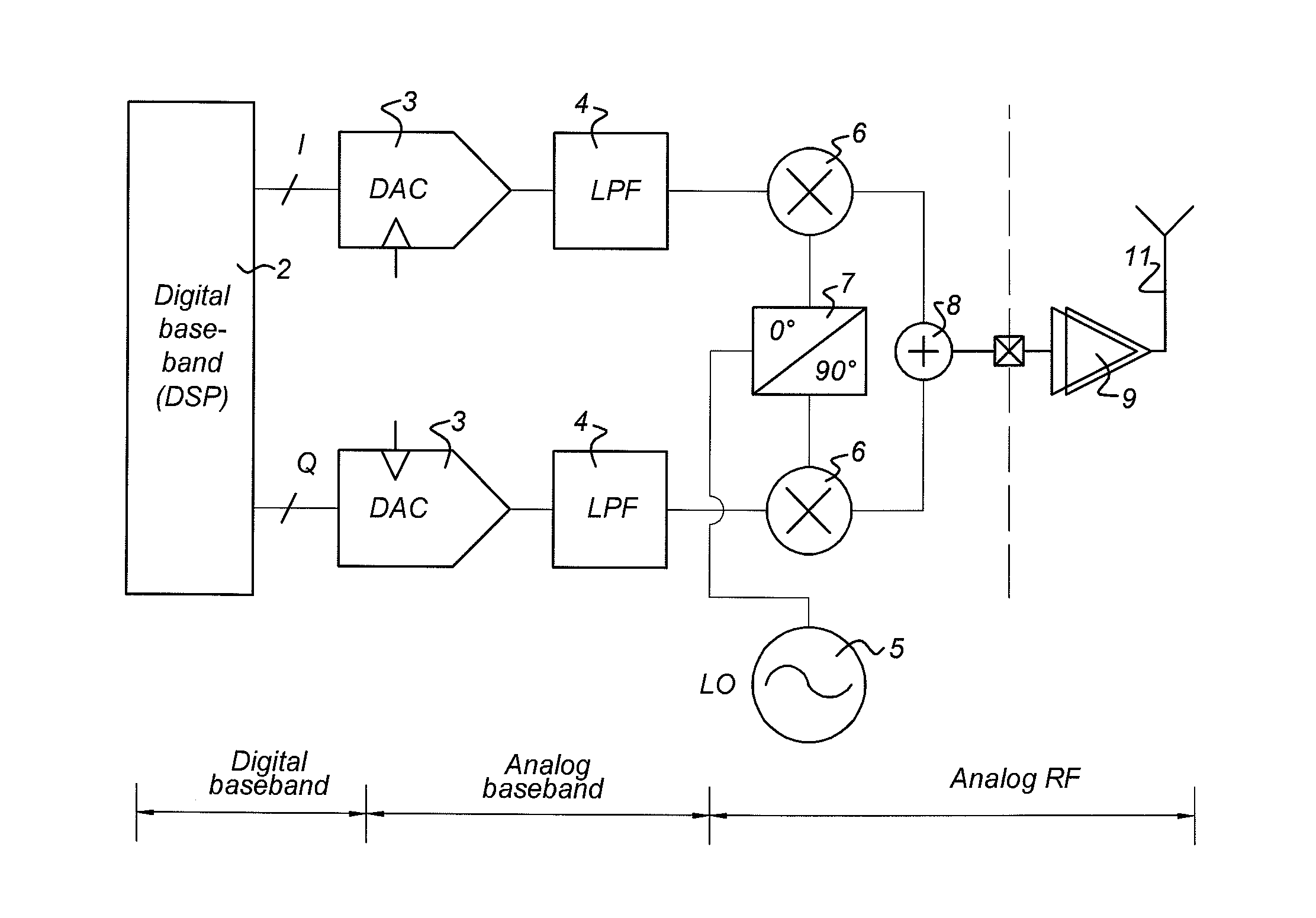
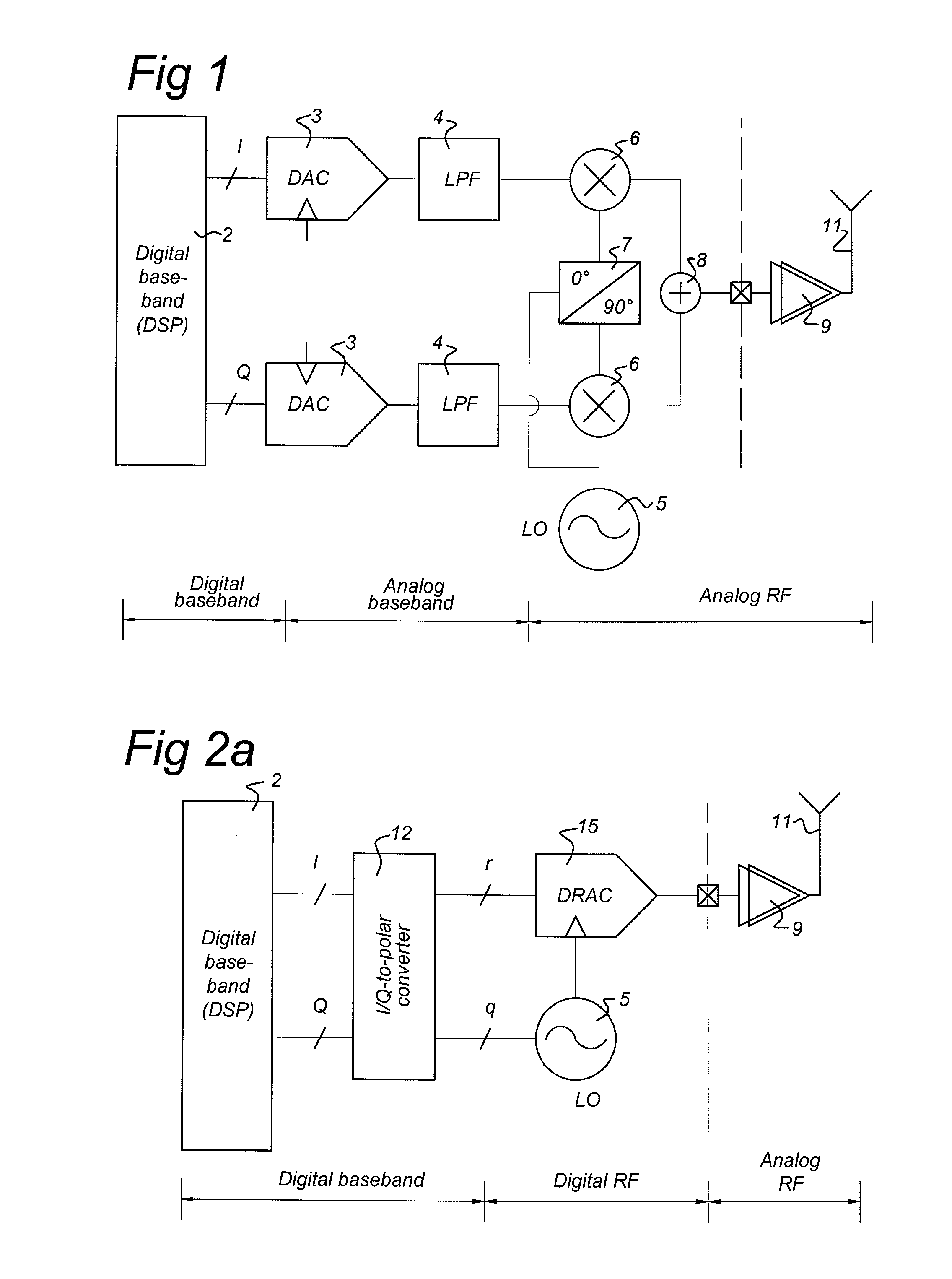
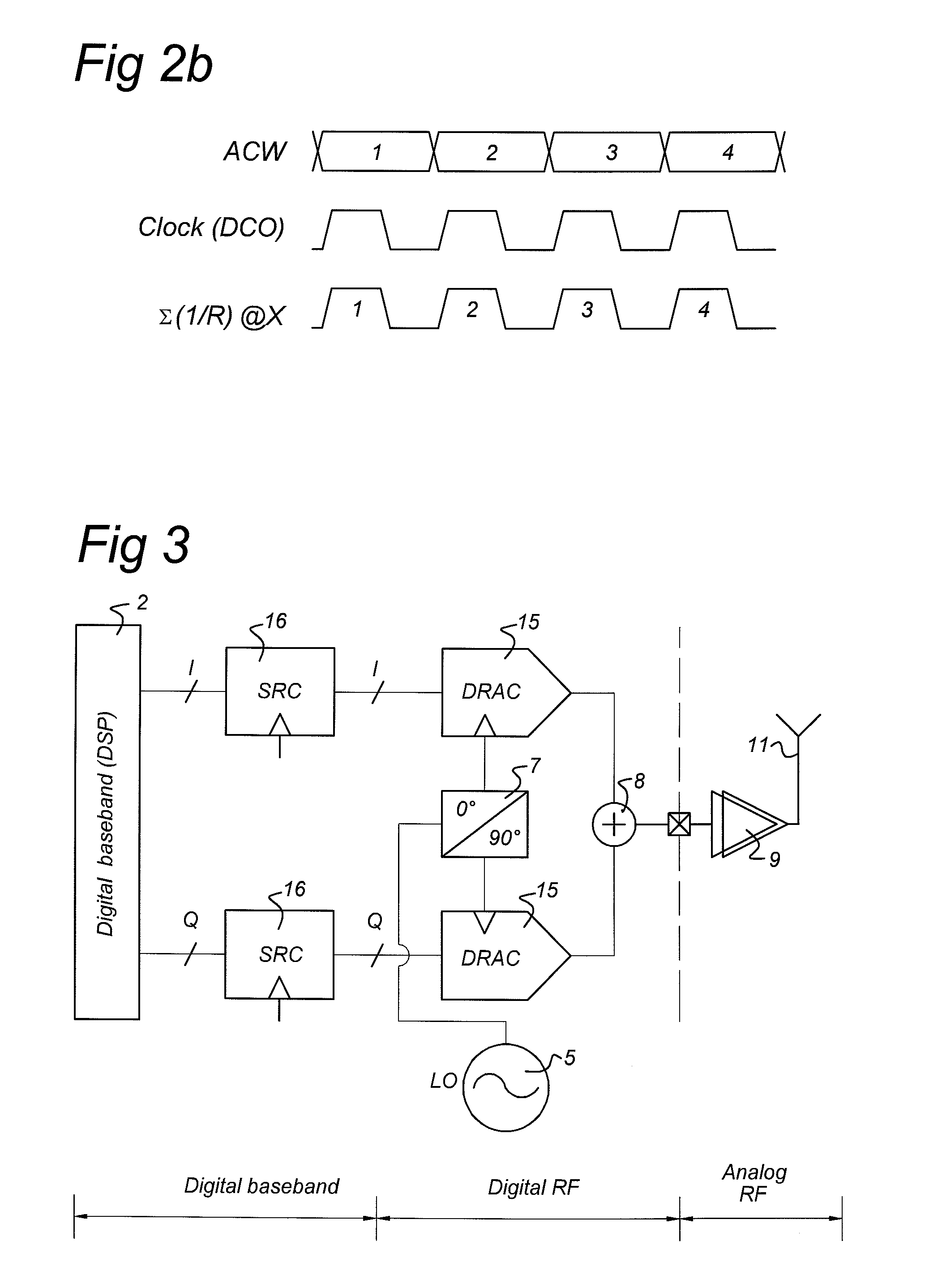
[0055]Embodiments of the invention relates to a method and system for (digitally) generating a radio-frequency (RF) signal to be transmitted. In accordance with embodiments of the invention, this is accomplished without any intermediate stages or without resorting to polar topology.

[0056]Polar transmitter (TX) topology is a known solution that involves power amplifiers (PA). However, this technique is only proven so far for narrowband systems, and it cannot be readily used for wideband modulation schemes, such as those in WiMAX and 3GPP LTE.

[0057]Embodiments of the invention can be applied in all RF transmission systems, e.g. wireless connectivity, cell phones and base stations. Cell phones or basestations can be achieved using the present invention that feature higher integration levels, better power efficiency (hence longer battery lifetime), and more sophisticated reconfigurability. They can be also advantageously used with antenna arrays, where advantages in the cost, size, powe...


PUM


Abstract

An electronic circuit, such as a transmitter, for receiving a modulating signal including an in-phase component (I) and a quadrature component (Q). The electronic circuit has a first digital-to-RF-amplitude convertor (DRAC) receiving the in-phase component and a second digital-to-RF-amplitude convertor (DRAC) receiving the quadrature component. The first digital-to-RF-amplitude convertor is operative in a first duty cycle that is different from 50% and the second digital-to-RF-amplitude convertor is operative in a second duty cycle that is different from 50% and substantially the same in value as said first duty cycle.

Description

CROSS-REFERENCE TO RELATED APPLICATIONS[0001]The present application claims priority under 35 U.S.C. §119 to Dutch Patent Application No. 2003880 (filed on Nov. 30, 2009), which is hereby incorporated by reference in its entirety.FIELD OF THE INVENTION[0002]Embodiments of the invention relate to an electronic circuit, such as a digital power amplifier as part of a transmitter, for receiving a modulating signal including an in-phase component (I) and a quadrature component (Q), the electronic circuit comprising a first digital-to-RF-amplitude convertor (DRAC) receiving the in-phase component and a second digital-to-RF-amplitude convertor (DRAC) receiving the quadrature component.BACKGROUND OF THE INVENTION[0003]A. Analog-Intensive RF Transmitters. Until around mid-1990's, virtually all monolithic radio frequency (RF) transmitters (TX) have been analog intensive and based on an architecture similar to that shown in the block diagram of FIG. 1. At the transmitter back-end, the baseband...

Claims


Application Information

Patent Timeline
Patent Type & Authority Applications(United States)
IPC IPC(8): H04L27/00
CPCH03F3/217H03F3/193
Inventor STASZEWSKI, BOGDANDE VREEDE, LEONARDUS CORNELIS NICOLAAS
Owner TECH UNIV DELFT
Why Eureka
Try Eureka