

Organic light emitting diode device
- Summary
- Abstract
- Description
- Claims
- Application Information
AI Technical Summary
Benefits of technology
Problems solved by technology
Method used
Image

Examples
example 1-1
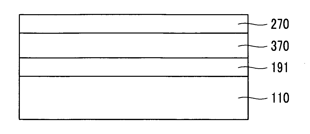
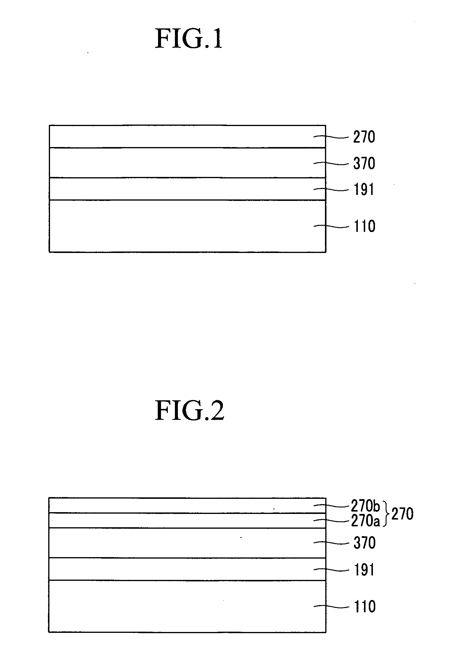
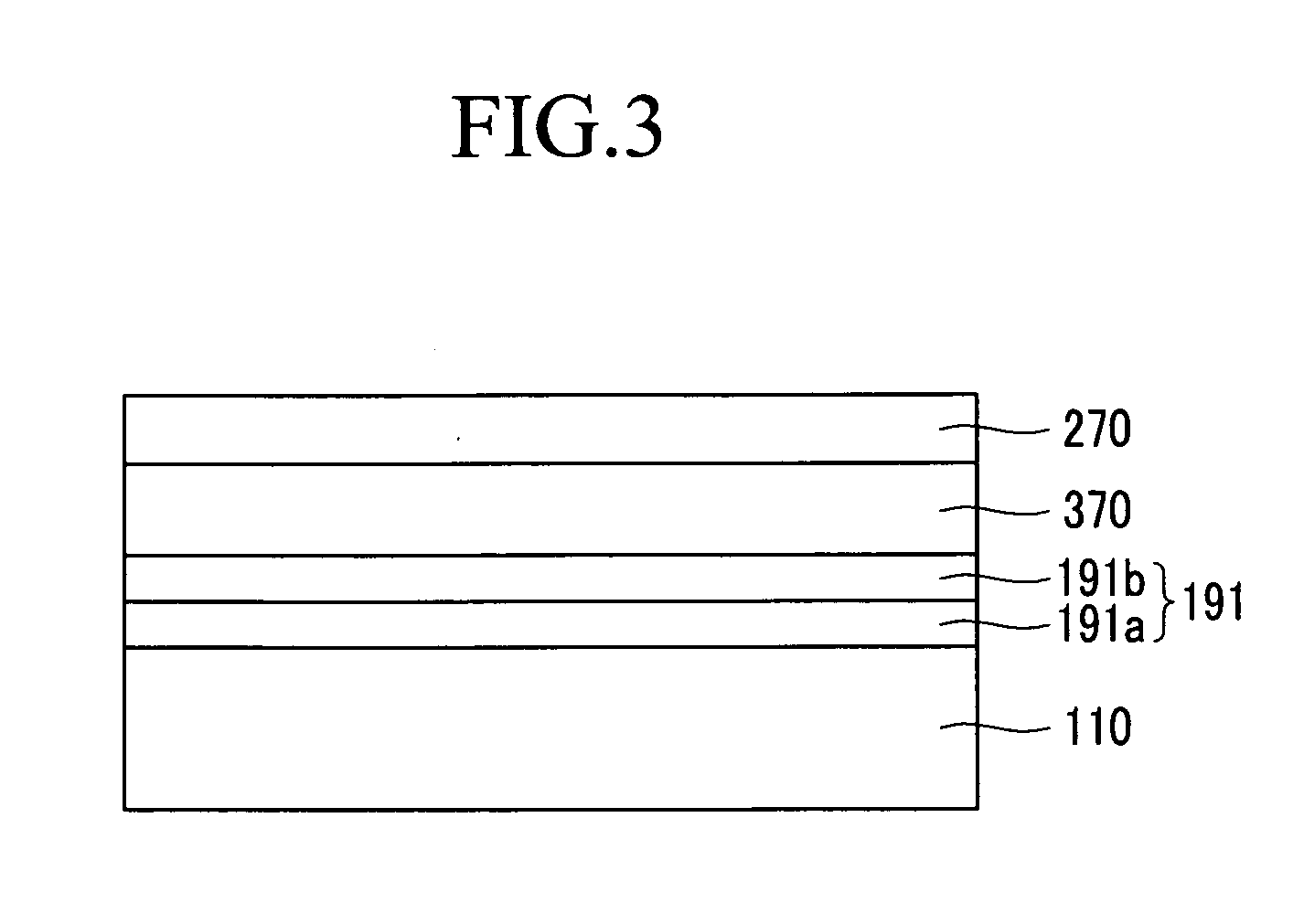
[0085]ITO was laminated on a glass substrate, followed by patterning to form a bottom electrode. Then, tris(8-hydroxyquinoline) aluminum (Alq3) was deposited as an electron transport layer. As an emitting layer, Alq3 doped with 1 wt % of coumarin 6 was co-deposited thereon. As a hole injection layer and a hole transport layer, N,N-dinaphthalene-1-yl-N,N-diphenyl-benzidine (NPB) was deposited. Then, a ytterbium (Yb)-silver (Ag) alloy was formed at a 5:1 ratio to a 100 Å thickness by thermal evaporation to form a top electrode.
example 1-2
[0086]An organic light emitting element was fabricated according to the same method as in Example 1-1, except that the ytterbium (Yb)-silver (Ag) alloy was formed at a 3:1 ratio instead of 5:1 ratio.
example 1-3
[0087]An organic light emitting element was fabricated according to the same method as in Example 1-1, except that the ytterbium (Yb)-silver (Ag) alloy was formed at a 2:1 ratio instead of 5:1 ratio.
PUM
 Abstract
Description
Claims
Application Information