
Low damage photoresist strip method for low-k dielectrics

a dielectric and photoresist strip technology, applied in the direction of lighting and heating apparatus, cleaning using liquids, instruments, etc., can solve the problems of high oxidizing conditions, general unsuitability for low-k materials, and unsuitability of conventional strip plasma conditions

Inactive Publication Date: 2011-06-16
NOVELLUS SYSTEMS
View PDF41 Cites 92 Cited by
  • Summary
  • Abstract
  • Description
  • Claims
  • Application Information

AI Technical Summary

Benefits of technology

[0007]In certain embodiment, the methods involve introducing gas comprising a weak oxidizing agent, fluorine-containing compound and hydrogen into the reaction chamber, and applying RF power to form a plasma within the reaction chamber to convert at least a portion of the material to gaseous form, thereby removing at least a portion of the material from the partially fabricated integrated circuit. As stated previously, methods may be used to remove photoresist and / or residues from the etch process. Methods may be effectively implemented on Damascene devices, including single and dual Damascene devices.
[0008]According to various embodiments, the weak oxidizing agent comprises at least one of carbon dioxide, carbon monoxide, nitrous oxide, nitric oxide and nitrogen dioxide and water. In a particular embodiment, the weak oxidizing agent comprises carbon dioxide. In certain embodiments, the gas comprises between about 0.1% to about 10.0% carbon dioxide by volume. In some embodiments, the gas further comprises at least one inert carrier gas such as helium, argon or nitrogen. In certain embodiments, the gas does not comprise molecular oxygen.

Problems solved by technology

Highly oxidizing conditions are also generally unsuitable for use on low dielectric constant (low-k) materials.
As processes used to fabricate integrated circuits moves toward smaller and smaller dimensions and requires the use of dielectric materials having lower and lower dielectric constants, it has been found that the conventional strip plasma conditions are not suitable.

Method used


Image

  • Low damage photoresist strip method for low-k dielectrics
  • Low damage photoresist strip method for low-k dielectrics
  • Low damage photoresist strip method for low-k dielectrics

Examples


Embodiment Construction

Introduction

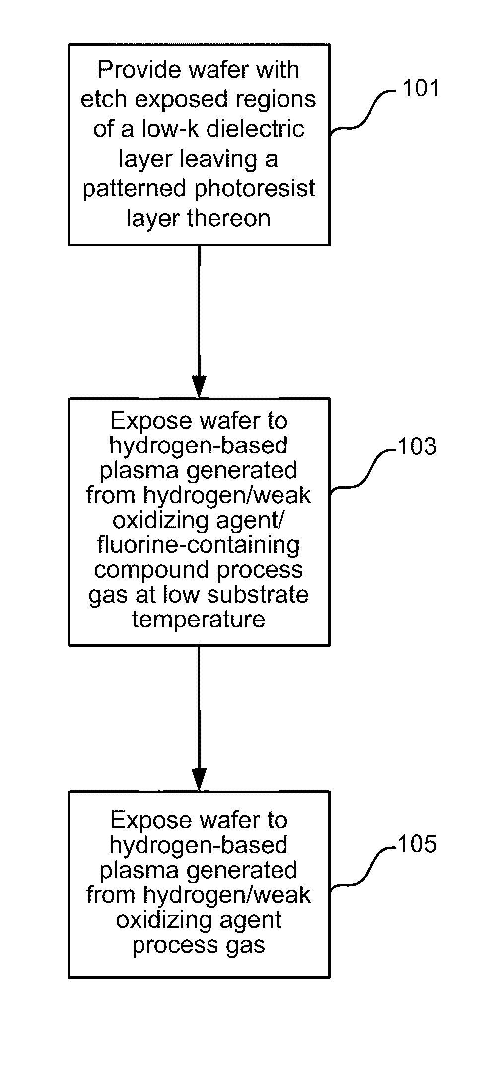
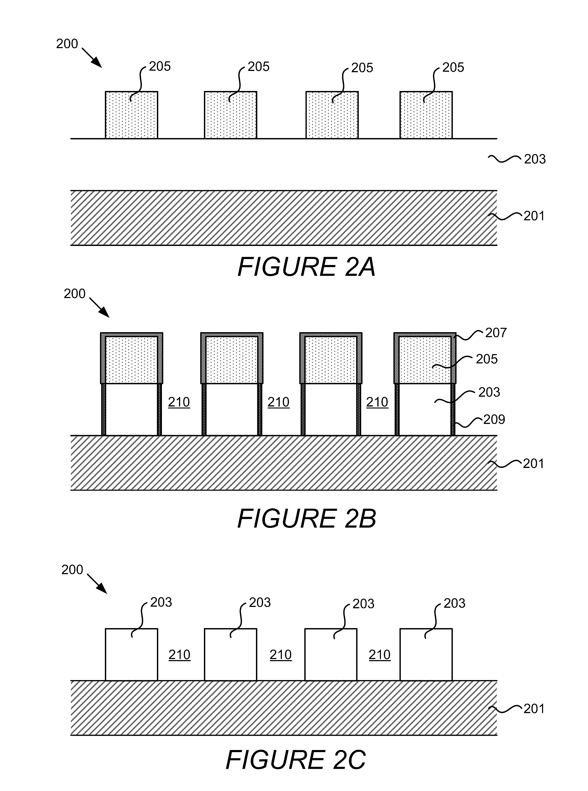
[0020]In the following detailed description of the present invention, numerous specific embodiments are set forth in order to provide a thorough understanding of the invention. However, as will be apparent to those skilled in the art, the present invention may be practiced without these specific details or by using alternate elements or processes. In other instances well-known processes, procedures and components have not been described in detail so as not to unnecessarily obscure aspects of the present invention.

[0021]In this application, the terms “semiconductor wafer”, “wafer” and “partially fabricated integrated circuit” will be used interchangeably. One skilled in the art would understand that the term “partially fabricated integrated circuit” can refer to a silicon wafer during any of many stages of integrated circuit fabrication thereon. The following detailed description assumes the invention is implemented on a wafer. However, the invention is not so limited. Th...


PUM

PropertyMeasurementUnit
Temperatureaaaaaaaaaa

Abstract

Improved methods for stripping photoresist and removing etch-related residues from dielectric materials are provided. In one aspect of the invention, methods involve removing material from a dielectric layer using a hydrogen-based etch process employing a weak oxidizing agent and fluorine-containing compound. Substrate temperature is maintained at a level of about 160° C. or less, e.g., less than about 90° C.

Description

BACKGROUND[0001]The present invention pertains to methods for stripping photo-resist material and removing etch-related residues from the surface of a partially fabricated integrated circuit in preparation for further processing.[0002]Damascene processing techniques are often preferred methods in many modern integrated circuit manufacturing schemes because it requires fewer processing steps and offers a higher yield than other methods. Damascene processing involves forming metal conductors on integrated circuits by forming inlaid metal lines in trenches and vias in a dielectric layer (inter-metal dielectric). As part of the Damascene process, a layer of photoresist is deposited on a dielectric layer. The photoresist is a light-sensitive organic polymer which can be “spun on” in liquid form and dries to a solid thin film. The photosensitive photoresist is then patterned using light through the mask and wet solvent. A plasma etching process (dry etch) is then used to etch exposed port...

Claims


Application Information

Patent Timeline
IPC IPC(8): B08B5/00B08B13/00C23F1/08
CPCG03F7/427H01L21/31058H01L21/67207H01L21/02046H01L21/02315H01L21/3065H01L21/76807
Inventor CHEUNG, DAVIDLI, TEDGUHA, ANIRBANOSTROWSKI, KIRK
Owner NOVELLUS SYSTEMS
Learn More