Solar Cell and Manufacturing Method Thereof

a manufacturing method and solar cell technology, applied in the field of solar cells, can solve the problems of warpage of aluminum and silicon linear expansion coefficients, increase in manufacturing costs, so as to reduce manufacturing costs, reduce power energy consumption, and simplify the manufacturing process

Inactive Publication Date: 2011-06-16
MITSUBISHI ELECTRIC CORP
View PDF4 Cites 30 Cited by
  • Summary
  • Abstract
  • Description
  • Claims
  • Application Information

AI Technical Summary

Benefits of technology

[0019]With the method of manufacturing a solar cell according to the present invention, the electrodes and a high-concentration region in which impurities of the first conductive type are diffused in high concentration can be formed at a time by one firing process. Hence, the manufacturing process can be simplified, the amount of power energy consumption can be reduced, and thereby the manufacturing costs can be reduced. Thus, an excellent solar cell with no warpage and with excellent battery cell characteristics can be produced at low costs.

Problems solved by technology

In the meantime, concerns are rising that silicon materials could become in short because of prospective rapid growth of silicon solar batteries.
However, if the thickness of the silicon substrate is to be reduced, during the firing operation for electrode formation in the above process, the difference between the linear expansion coefficients of aluminum and silicon incurs warpage at the time of cooling in a subsequent stage in the firing operation.
This significantly increases the breakage rate of solar cells during the manufacturing process.
However, if the thickness of the aluminum paste is too small, the thickness of the BSF layer that is formed by firing also becomes small, which prevents the solar cell from maintaining its characteristics.
However, because the aluminum back electrodes formed of aluminum has a low reflectance with respect to the long-wavelength light, the utilization efficiency decreases and the amount of current generation is lessened.
With this method also, the number of steps is significantly increased, and thus volume production of solar cells cannot be efficiently performed.

Method used


Image

  • Solar Cell and Manufacturing Method Thereof
  • Solar Cell and Manufacturing Method Thereof
  • Solar Cell and Manufacturing Method Thereof

Examples


first embodiment

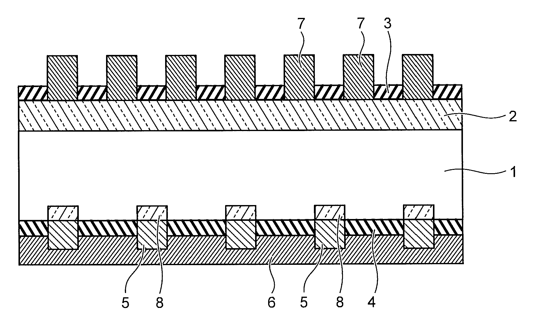
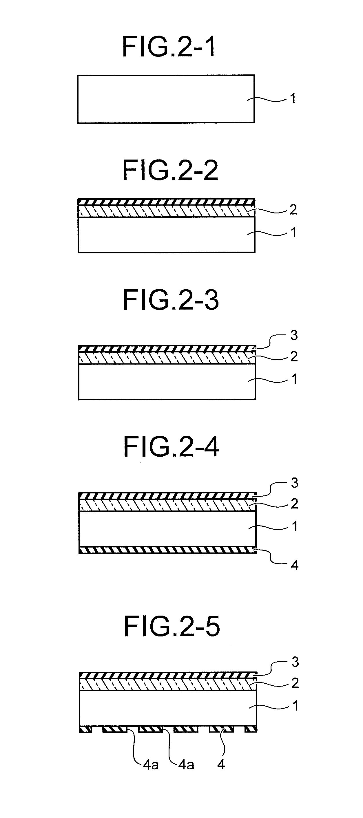
[0055]FIG. 1 is a section view explaining a structure of a solar cell according to a first embodiment of the present invention. In the solar cell according to the present embodiment, an impurity diffusion layer (n-type impurity diffusion layer) 2 is formed by phosphorus diffusion on the light receiving surface of a semiconductor substrate 1 of p-type silicon, and an antireflective film 3 is formed of a silicon nitride film.

[0056]For the semiconductor substrate 1, a p-type single-crystalline or polycrystalline silicon substrate may be used. The substrate, however, is not limited thereto, and an n-type silicon substrate may be adopted. Furthermore, a silicon oxide film may be adopted for the antireflective film 3. In addition, fine unevenness is formed as a texture structure in the surface of the semiconductor substrate 1 of the solar cell on the light receiving surface side. The fine unevenness is configured to increase the area for absorbing external light on the light receiving sur...

second embodiment

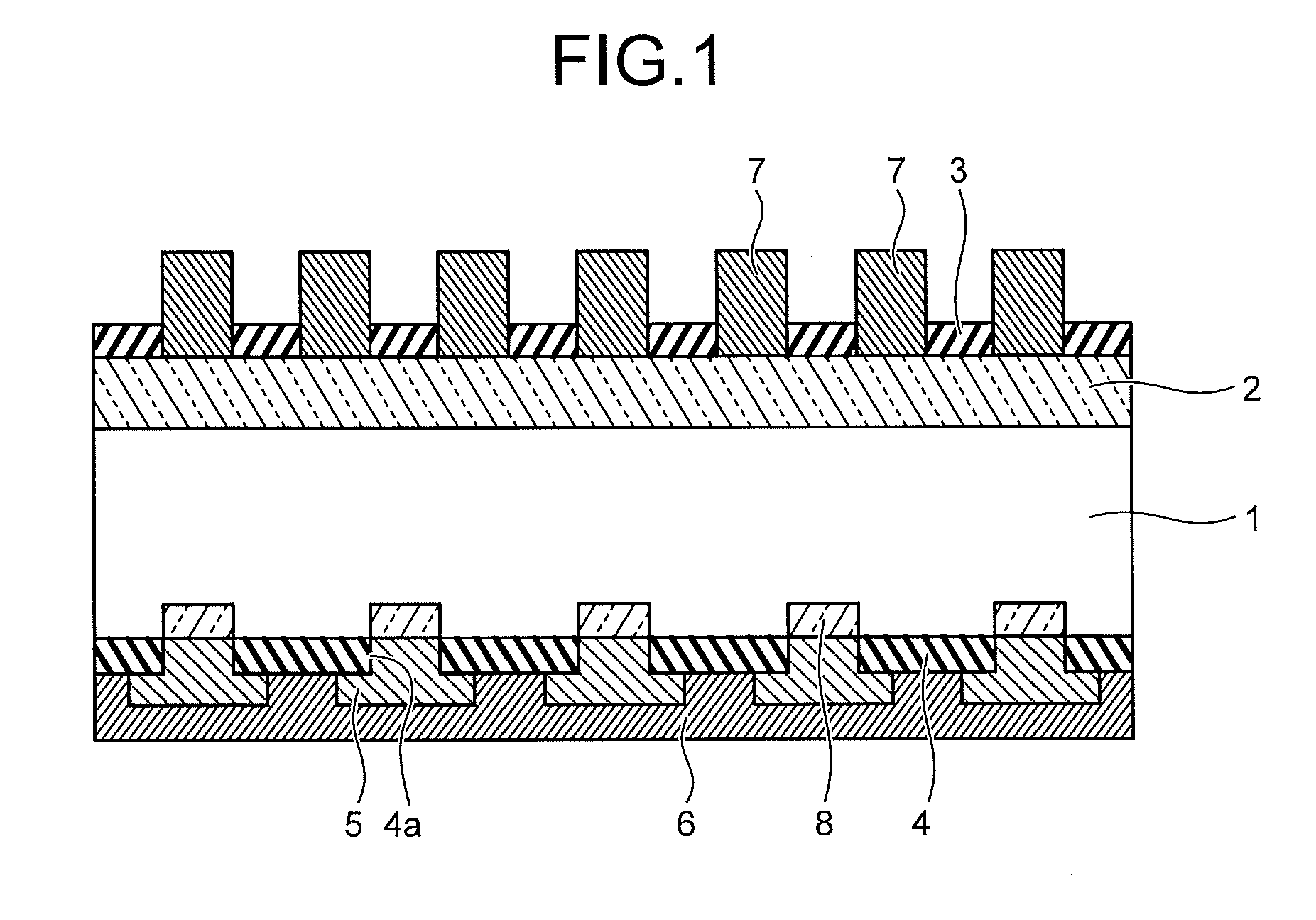
[0074]In the second embodiment, another solar cell and manufacturing method thereof in the present invention are explained in detail. FIG. 4 is a section view explaining a structure of the solar cell according to the second embodiment. Portions of the structure that are the same as the first embodiment are given the same numerals as in FIG. 1, and thereby the detailed explanation is omitted.

[0075]In the solar cell according to the present embodiment, the impurity diffusion layer (n-type impurity diffusion layer) 2 is formed by phosphorus diffusion on the light receiving surface of the p-type silicon semiconductor substrate 1, and also the antireflective film 3 of a silicon nitride film is formed thereon. Fine unevenness is formed as a texture structure in the light receiving surface of the semiconductor substrate 1 of the solar cell. The fine unevenness has a structure that increases the area of the light receiving surface that absorbs external light, suppresses the reflectance on t...


PUM

PropertyMeasurementUnit
thicknessaaaaaaaaaa
temperatureaaaaaaaaaa

Abstract

Forming an impurity diffusion layer of the second conductivity type and an antireflective film on one surface side of a semiconductor substrate of the first conductivity type; applying the first electrode material onto the antireflective film; forming a passivation film on the other surface side of the semiconductor substrate; forming openings in the passivation film to reach the other surface side; applying a second electrode material containing impurity elements of the first conductive type to fill the openings and not to be in contact with the second electrode material of adjacent openings; applying a third electrode material onto the passivation film to be in contact with the entire second electrode material; forming at a time, by heating the semiconductor substrate at a predetermined temperature after applying the first electrode material and the third electrode material, the first electrodes, a high-concentration region, and the second electrodes and third electrode.

Description

TECHNICAL FIELD[0001]The present invention relates to a solar cell and a manufacturing method thereof, and especially to a solar cell that has less warpage of the solar battery and exhibits excellent characteristics even when the substrate is thinned, and a solar cell manufacturing method with which such a solar cell can be efficiently produced.BACKGROUND ART[0002]Aluminum paste that has been conventionally adopted for aluminum back electrodes of a photovoltaic device such as a solar battery has an advantage that the electrodes can be readily formed by screen printing or the like. Furthermore, the aluminum paste has another advantage that a so-called back surface field (BSF) layer, which improves the efficiency of collecting majority carriers, can be readily formed by diffusing aluminum into the silicon substrate and thereby readily forming by heat treatment a p+ layer in which p-type impurities are diffused in high concentration, and generating a barrier electric field inside the p...

Claims


Application Information

Patent Timeline
Patent Type & Authority Applications(United States)
IPC IPC(8): H01L33/44
CPCH01L31/022425Y02E10/547H01L31/02167H01L31/1804H01L31/0504H01L31/068Y02P70/50
Inventor HAMA, ATSUROMORIKAWA, HIROAKI
Owner MITSUBISHI ELECTRIC CORP
Why Eureka
Try Eureka