[0013]The present invention has been conceived in view of the above problems, and an object of the invention is to provide a method of manufacturing a multilayer wiring substrate which can set the degree of surface roughness of the outermost layer to a proper level. Another object of the present invention is to provide a multilayer wiring substrate in which the degree of surface roughness of the outermost layer is set to a proper level, to thereby enable an IC
chip to be mounted thereon reliably.
[0015]According to the invention described in the first means, the outermost resin insulation layer is formed of the same resin insulation material as the inner resin insulation layers of the laminate structure. Therefore, as compared with the case where the outermost resin insulation layer is formed of a different resin insulation material, the influence of a difference in coefficient of
thermal expansion in the laminate structure can be mitigated. As a result, warpage of the multilayer wiring substrate can be suppressed. Since the outermost resin insulation layer is formed of the same resin insulation material as the inner resin insulation layers, it is difficult to form openings by a
lithography process. However, openings can be reliably formed in the outermost resin insulation layer through performance of
laser drilling. Furthermore, the desmear step is performed after the build-up step, the degree of surface roughness of the outermost resin insulation layer can be set to an arbitrary level. Accordingly, the surface of the outermost resin insulation layer, which constitutes the multilayer wiring substrate, can have a surface roughness suitable to flux and underfill agent, whereby they can be spread in a proper state by their wettability.
[0018]There may be successively performed a connection-terminal forming step of, after the base-material removing step, forming the second-main-surface-side connection terminals in a state in which
etching resist films cover an entirety of the first main surface and the
metal foil in a predetermined pattern corresponding to the second-main-surface-side connection terminals, and subsequently
etching the
metal foil to form the second-main-surface-side connection terminals; and a resist removing step of removing the etching resist films to thereby
expose the first-main-surface-side connection terminals and the second-main-surface-side connection terminals. In this method, the step of forming openings through
laser drilling is performed before performance of the base-material removing step. In this case, since the laminate structure on the base material has a relatively large strength, it can be maintained in a warpage-
free state, whereby openings can be formed on the surface of the laminate structure at accurate positions.
[0020]The drilling step my be performed such that the first-main-surface-side connection terminals are exposed, and a portion of one of the plurality of conductive layers other than the first-main-surface-side connection terminals is exposed. Specifically, for example, a portion of a conductive layer which will become an alignment mark may be exposed, whereby positioning of the wiring substrate is facilitated.
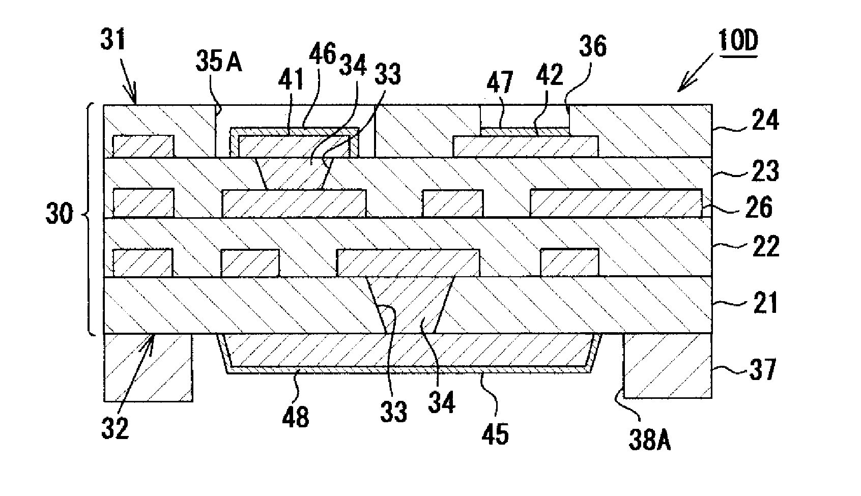
[0022]According to the invention described in the second means, the multilayer wiring substrate is formed such that a plurality of resin insulation layers made primarily of the same resin insulation material, and a plurality of conductive layers are laminated alternately, and assumes the form of a coreless wiring substrate having no substrate core. In this multilayer wiring substrate, the outermost resin insulation layer is formed of a resin insulation material which is the same as that used for forming the inner resin insulation layers and which is not photocurable, as compared with the case where the outermost resin insulation layer is formed of a different resin insulation material, the influence of a difference in coefficient of
thermal expansion can be mitigated. As a result, warpage of the multilayer wiring substrate can be suppressed. Furthermore, two types of connection terminals, including IC-
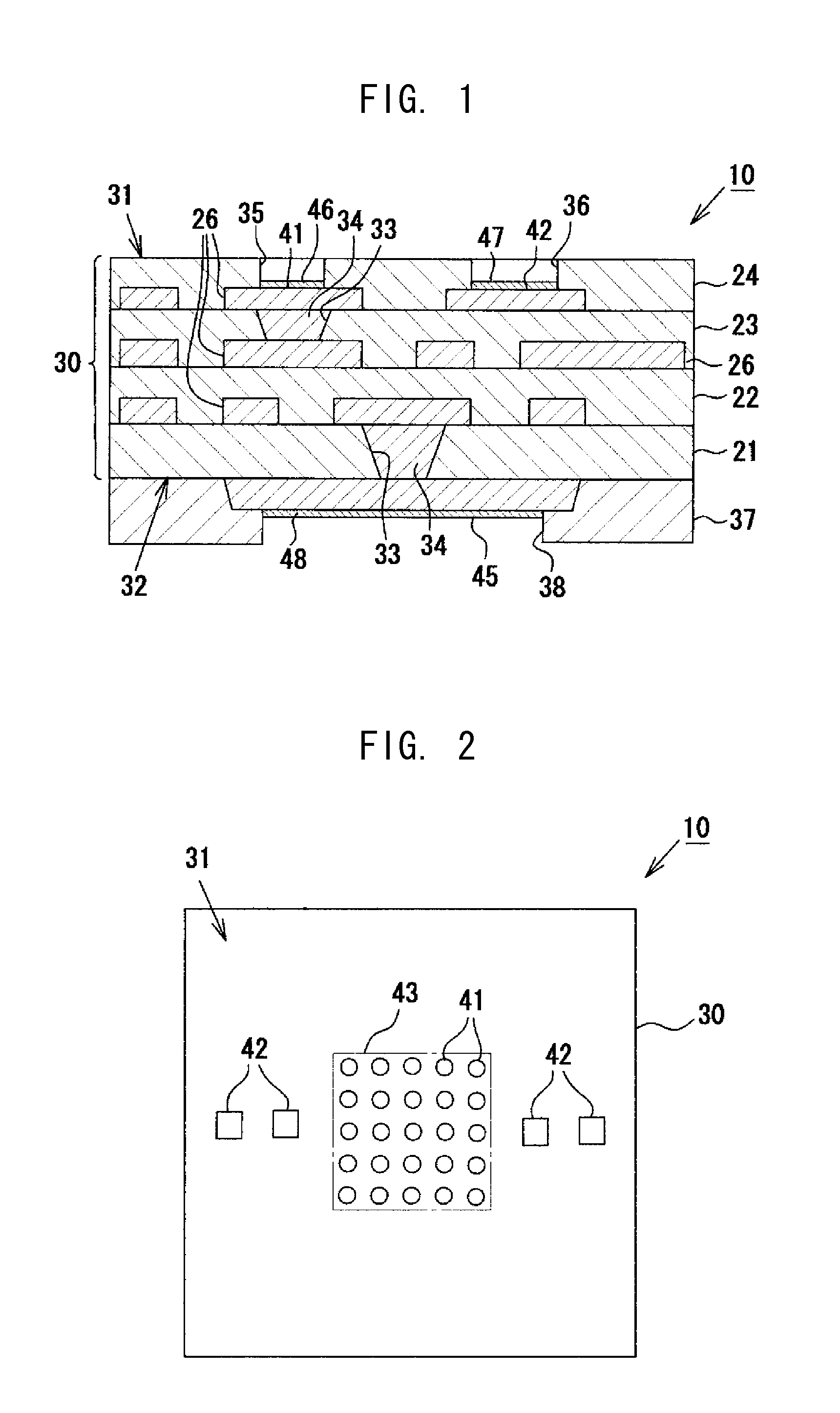
chip connection terminals to which an IC chip is to be connected, and passive-component connection terminals to which a passive component connection is to be connected and which is larger in area than the IC-chip connection terminals, are present on the first main surface as the first-main-surface-side connection terminals; and the IC-chip connection terminals are disposed in the plurality of openings. The top surfaces of the IC-chip connection terminals are lower in height than the surface of the outermost resin insulation layer, and
peripheral portions of the IC-chip connection terminals are buried in the outermost resin insulation layer. Accordingly, the outermost resin insulation layer functions as a solder resist film, whereby solder bumps can be reliably formed on the top surfaces of the IC-chip connection terminals. Moreover, since the outermost resin insulation layer is formed of a build-up material which is the same as that used to form the inner resin insulation layers and which is excellent in electrical insulation performance, the intervals of the IC-chip connection terminals can be narrowed, whereby the degree of integration of the multilayer wiring substrate can be increased.
[0023]Preferably, each of the passive-component connection terminals has a structure in which a plating layer of a material other than
copper covers a top surface and a side surface of a portion of a
copper layer which portion is a main constituent of the passive-component connection terminal, and each of the IC-chip connection terminals has a structure in which a plating layer of a material other than
copper covers only a top surface a portion of the copper layer which portion is a main constituent of the IC-chip connection terminal. This configuration enables reliable formation of relatively large filets on the top and side surfaces of the passive-component connection terminals. Also, solder bumps can be reliably formed on the top surfaces of the IC-chip connection terminals. The inter-terminal spacing of the passive-component connection terminals is greater than that of the IC-chip connection terminals, and the passive-component connection terminals have a relatively
large size. Therefore, passive components can be reliably solder-connected to the passive-component connection terminals with a sufficiently large strength via filets formed on the top and side surfaces of the passive-component connection terminals. Meanwhile, since the inter-terminal spacing of the IC-chip connection terminals is small, if solder bumps bulge from the side surfaces of the IC-chip connection terminals, a short-circuit may be formed between the terminals. In contrast, in the present invention, since solder bumps are formed only on the top surfaces of the IC-chip connection terminals, solder bumps do not bulge laterally, whereby formation of a short-circuit between the terminals can be avoided.

