Method for manufacturing group iii nitride semiconductor layer, method for manufacturing group iii nitride semiconductor light-emitting device, and group iii nitride semiconductor light-emitting device, and lamp

a technology of nitride and semiconductor, which is applied in the direction of solid-state devices, vacuum evaporation coatings, coatings, etc., can solve the problem of inability to perform an additional test by third parties, and achieve the effect of easy control of the electric resistance in the group iii nitride layer, and easy control of the amount of si

Inactive Publication Date: 2011-07-07
TOYODA GOSEI CO LTD
View PDF9 Cites 10 Cited by
  • Summary
  • Abstract
  • Description
  • Claims
  • Application Information

AI Technical Summary

Benefits of technology

[0038]The method for manufacturing a Group III nitride semiconductor layer of the present invention is a method in which Si is supplied to a Group III nitride semiconductor layer by adding a hydride containing Si as a dopant to a gas for formation of a plasma, thereby supplying Si into a chamber when the Group III nitride semiconductor layer in which Si has been added as the dopant is formed by a reactive sputtering method. Therefore, it is possible to easily control the doping amount of Si by adjusting the additive amount of a Si hydride. When the Si hydride is used as a material of a Si element and is decomposed in the plasma, Si is less likely to be converted into the form of a multimer, and thus electric resistance in the Group III nitride layer can be decreased even if the concentration of the dopant is low.
[0039]As described above, since the dopant concentration of the Group III nitride semiconductor layer to be formed can be easily controlled, it becomes possible to optimally control electric resistance according to the objective properties and to stably form a Group III nitride semiconductor layer having satisfactory crystallinity on a substrate with high efficiency.
[0040]Since the method for manufacturing a Group III nitride semiconductor layer of the present invention is a method in which a Si hydride is added in a gas for formation of a first plasma, which contains no nitrogen element, to be introduced into a chamber in a first plasma generation step of generating a first plasma containing sputtering particles comprised of at least a Group III element, it is possible to efficiently dope Si.
[0041]As described above, since the method for manufacturing a Group III nitride semiconductor layer of the present invention can easily control the doping concentration of Si by adjusting the additive amount of the Si hydride and Si is less likely to be converted into the form of a multimer, Si has a high activation rate. Therefore, it is possible to optimally control electric resistance and to form a Group III nitride semiconductor layer having excellent crystallinity.
[0042]According to the method for manufacturing a Group III nitride semiconductor light-emitting device of the present invention, since an n-type semiconductor layer is formed by the manufacturing method described above, it is possible to obtain a Group III nitride semiconductor light-emitting device, that includes a Group III nitride semiconductor layer having satisfactory crystallinity with controlled electric resistance and also has excellent light emission properties.
[0043]Furthermore, since the Group III nitride semiconductor light-emitting device and the lamp of the present invention are obtained by the method for manufacturing a Group III nitride semiconductor light-emitting device of the present invention, they include a Group III nitride semiconductor layer having satisfactory crystallinity with controlled electric resistance and also have excellent light emission properties.

Problems solved by technology

Non-Patent Document 3 does not describe a specific doping method and therefore it is impossible to perform an additional test by third party.

Method used


Image

  • Method for manufacturing group iii nitride semiconductor layer, method for manufacturing group iii nitride semiconductor light-emitting device, and group iii nitride semiconductor light-emitting device, and lamp
  • Method for manufacturing group iii nitride semiconductor layer, method for manufacturing group iii nitride semiconductor light-emitting device, and group iii nitride semiconductor light-emitting device, and lamp
  • Method for manufacturing group iii nitride semiconductor layer, method for manufacturing group iii nitride semiconductor light-emitting device, and group iii nitride semiconductor light-emitting device, and lamp

Examples


examples

[0206]The present invention will be described in more detail by way of Example, but the present invention is not limited only to these Examples.

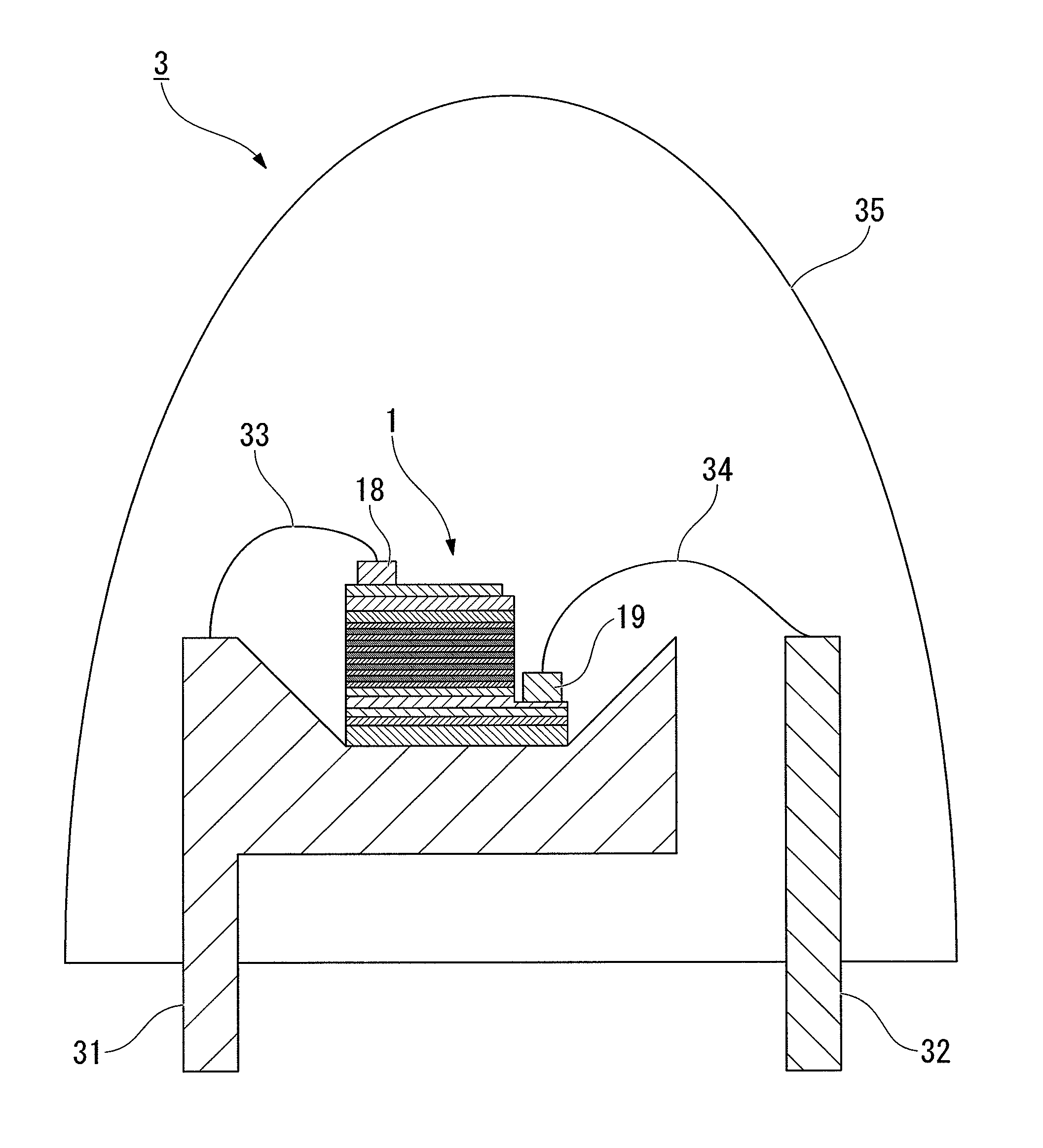
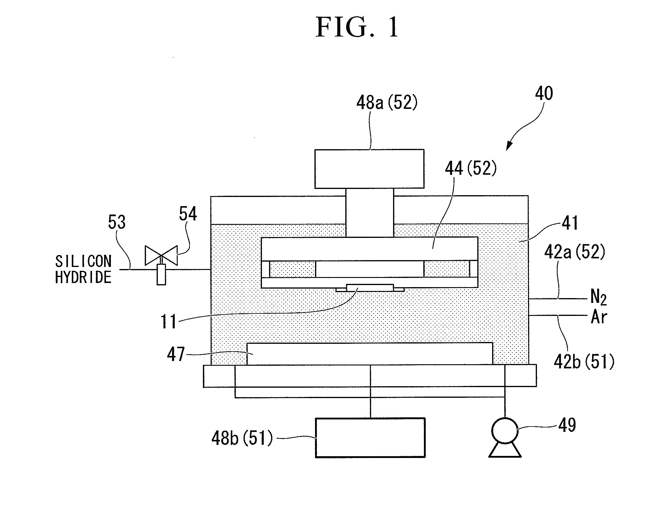
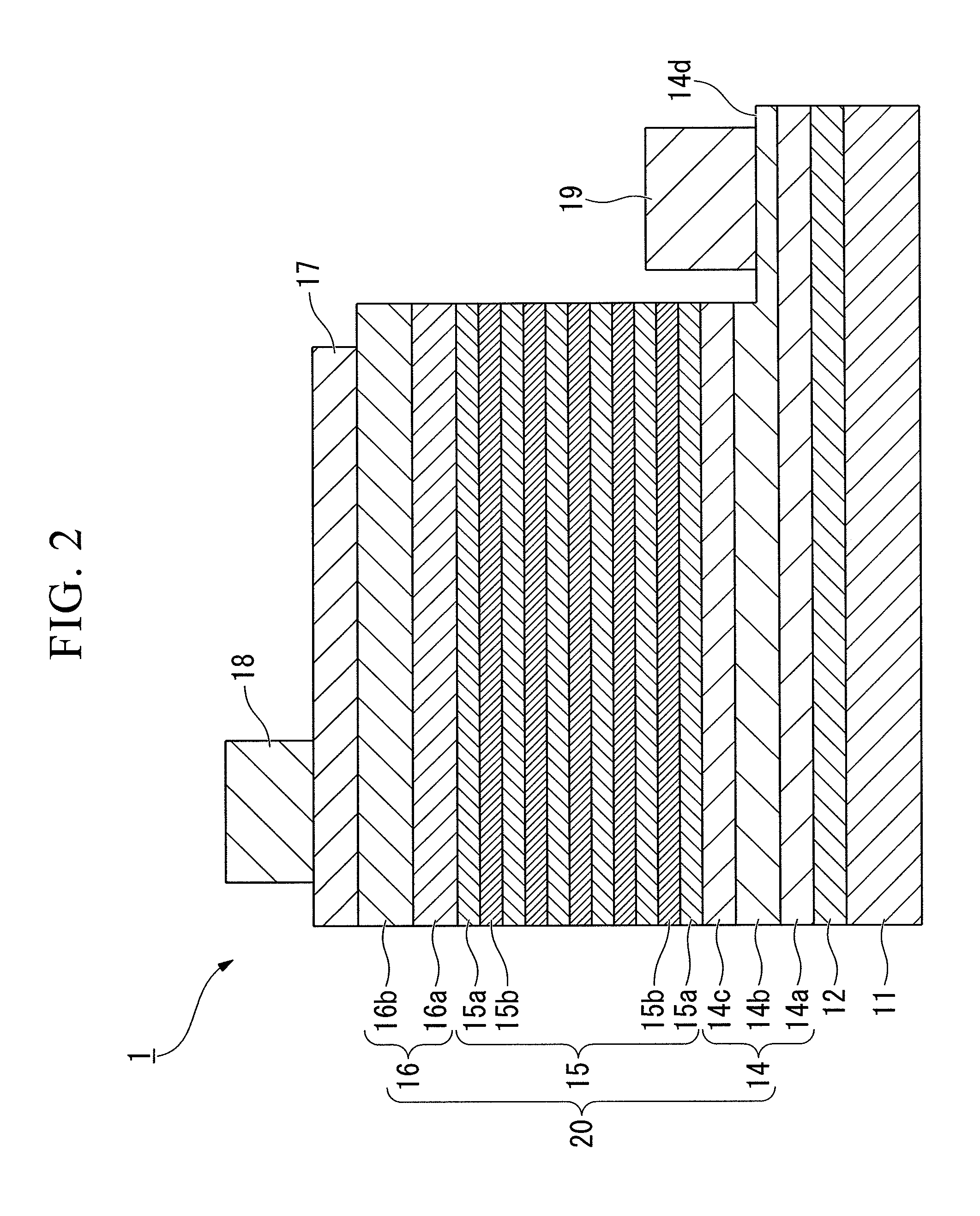
[0207]In order to examine a relation between the flow rate of a silane gas (SiH4) and the amount of Si, with which a GaN layer is doped, an n-type semiconductor layer 14 shown in FIG. 4 was formed in the following manner using a manufacturing method using a sputtering apparatus 40 shown in FIG. 1.

(Method for Manufacturing Samples of Test Examples)

[0208]First, a buffer layer 12 composed of AlN having a single crystal structure was formed on the c-plane of a substrate 11 composed of sapphire using a sputtering apparatus 40 shown in FIG. 1, and a ground layer 14a composed of an undoped GaN layer of an n-type semiconductor layer 14 and an n-type contact layer 14b composed of a Si-doped GaN layer of an n-type semiconductor layer 14 were sequentially laminated thereon.

[0209]More specifically, first, a substrate 11 composed of a 2-inch diameter (00...


PUM

PropertyMeasurementUnit
thicknessaaaaaaaaaa
thicknessaaaaaaaaaa
thicknessaaaaaaaaaa

Abstract

A method for manufacturing a Group III nitride semiconductor layer according to the present invention includes a sputtering step of disposing a substrate and a target containing a Group III element in a chamber, introducing a gas for formation of a plasma in the chamber and forming a Group III nitride semiconductor layer added with Si as a dopant on the substrate by a reactive sputtering method, wherein a Si hydride is added in the gas for formation of a plasma.

Description

TECHNICAL FIELD[0001]The present invention relates to a method for manufacturing a Group III nitride semiconductor layer that is suitable for use in a light-emitting diode (LED), a laser diode (LD), an electronic device, or the like, and particularly to a method for manufacturing a Group III nitride semiconductor layer that is used for formation of a Group III nitride semiconductor layer in which a dopant has been added, a method for manufacturing a Group III nitride semiconductor light-emitting device, and a Group III nitride semiconductor light-emitting device, and a lamp.[0002]The present invention claims priority on Japanese Patent Application No. 2008-062597 filed on Mar. 12, 2008 in Japan, the contents of which are incorporated herein by reference.BACKGROUND ART[0003]A Group III nitride semiconductor possess a band gap of a direction transition type of energy corresponding to the visible light to the ultraviolet light region, and has an excellent level of light emission effici...

Claims


Application Information

Patent Timeline
Patent Type & Authority Applications(United States)
IPC IPC(8): H01L33/44C23C14/34C23C14/14C23C14/06H01L21/203H01L33/06H01L33/32H01L33/42
CPCC23C14/0617H01L21/0237H01L2224/73265H01L2224/49107H01L2224/48257H01L2224/48247H01L2224/48091H01L2224/32245H01L33/007H01L21/02631H01L21/02576H01L21/02458H01L21/0254H01L2924/00014H01L2924/00H01L2924/181
Inventor YOKOYAMA, YASUNORIMIKI, HISAYUKI
Owner TOYODA GOSEI CO LTD
Why Eureka
Try Eureka