Optical semiconductor device and pumping light source for optical fiber amplifier

a technology of optical fiber amplifier and optical semiconductor, which is applied in the direction of solid-state devices, semiconductor lasers, lasers, etc., can solve the problems of thermal saturation of light output and discontinuous point (kink) in the light-current output characteristics, increase of threshold current, and difficulty in reducing the operation of anodes, so as to reduce the anode current and improve the current constrictivity , the effect of reducing the anode curren

Active Publication Date: 2011-07-07
FURUKAWA ELECTRIC CO LTD
View PDF5 Cites 16 Cited by
  • Summary
  • Abstract
  • Description
  • Claims
  • Application Information

AI Technical Summary

Benefits of technology

[0027]Because the optical semiconductor device of the invention is arranged such that the distance W1 between the n-type current blocking layers composing the current blocking region is narrower than the width W2 of the p-type cladding layer contacting with the n-type current blocking layer, the semiconductor device in which a contact region of the p-type cladding layer and the p-type current blocking layer is reduced and the anode current in the thyristor structure is reduced may be realized. Still more, the semiconductor device having the current blocking region by which current constrictivity is improved and by which turn-on current is hardly generated may be realized by reducing the anode current.
[0028]Further, because the semiconductor device of the invention is arranged such that the difference W1-W2 between the distance W1 between the n-type current blocking layers and the width W2 of the p-type cladding layer contacting with the n-type current blocking layer is more than −0.5 μm and less than 0 μm, it is possible to realize the highly reliable and high-output operable optical semiconductor device that is not influenced by thermal saturation of light output otherwise caused by an increase of device resistance due to diffusion of impurity in the p-type cladding layer generated in the fabrication process.
[0029]Further, because the semiconductor device of the invention is arranged such that concentration of p-type impurity of the p-type current blocking layer is in a range from 1×1018 cm−3 to 1.2×1018 cm−3, the anode current in the current device layer may be cut and absorption of light by the p-type impurity is cut. Therefore, it is possible to realize the optical semiconductor device capable of performing the high-output operations even when driven with high-current.
[0030]Further, because the semiconductor device of the invention is arranged such that the material composing the n-type substrate is InP, the optical semiconductor device most suitable for communication wavelength band may be realized with low threshold current and high efficiency.
[0031]Further, because the semiconductor device of the invention is arranged such that the active layer has the quantum well structure, the semiconductor device that highly efficiently operates with the low threshold current may be realized. Further, the active layer has the strain super-lattice quantum well structure, the semiconductor device that operates more highly efficiently with the low threshold current may be realized.
[0032]Further, because the semiconductor device of the invention is arranged such that the width of the active layer is selected so as to meet the single-transverse mode operation across the light waveguide direction, the optical semiconductor device capable of performing the high-output operation with the low threshold current that is most suitable for an optical communication system may be realized.

Problems solved by technology

However, the leak current generated in the current blocking region of the semiconductor device having the buried hetero (BH) structure may become a cause that induces an increase of threshold current, thermal saturation of light output and discontinuous point (kink) in the light-current output characteristics.
The discontinuous point (kink) is problematic in particular because it remarkably drops high output and high temperature operations of the semiconductor device.

Method used


Image

  • Optical semiconductor device and pumping light source for optical fiber amplifier
  • Optical semiconductor device and pumping light source for optical fiber amplifier
  • Optical semiconductor device and pumping light source for optical fiber amplifier

Examples


first embodiment

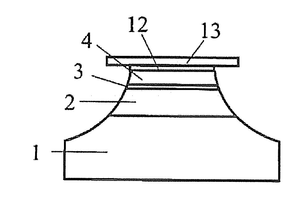
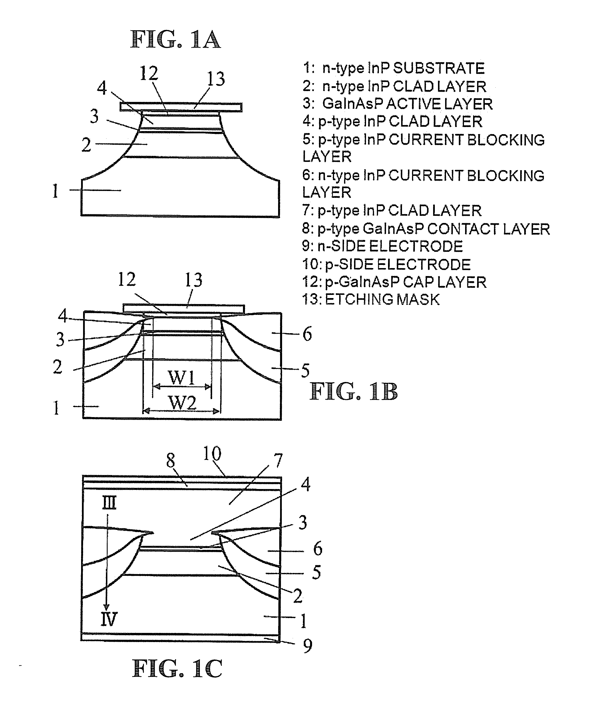
[0067]An embodiment of the invention will be explained next. After forming the n-type InP cladding layer 2 of 1 um thick, the GaInAsP active layer 3 and the p-type InP cladding layer 4 of 0.5 μm thick and the p-GaInAsP cap layer 12 of 0.05 μm thick whose compositional wavelength is 1.2 μm thick sequentially on the n-type InP substrate 1 in which sulfur (S) is doped as impurity at 670° C., the etching mask 13 composed of the SiNx dielectric film is formed on the p-GaInAsP cap layer 12 of the stripe to form the mesa-stripe by using wet etching. In forming the mesa-stripe, the mesa is formed so as to have the curved shape by which no specific plane orientation appears. The GaInAsP active layer 3 is composed of the multiple quantum well structure composed of five layers of GaAsP compressed strain quantum well layer of 4 nm thick whose lattice mismatching degree is around 1% and a GaInAsP barrier layer of 10 nm thick whose compositional wavelength is 1.2 μm and six layers of multistage o...


PUM


Abstract

A semiconductor device of the invention is formed so that n-type InP current blocking layers enter the inside of p-type InP cladding layers, i.e., the n-type current blocking layers ride over the upper part of the p-type InP cladding layers, so that a distance between the n-type InP current block layers composing a current blocking region is narrower than a width of the p-type cladding layers contacting with the n-type InP current blocking layers. Thereby, the semiconductor device whose leak current in the current blocking region may be reduced which permits high-output and high-temperature operations may be readily fabricated.

Description

BACKGROUND OF THE INVENTION[0001]1. Field of the Invention[0002]The present invention relates to an optical semiconductor device having a buried hetero-structure and to a pumping light source for optical fiber amplifier using the same.[0003]2. Description of the Related Art[0004]A current injection type semiconductor device adopts a structure having a current confinement function to efficiently inject current to an active layer, i.e., an emitting region. One of the current confinement structures uses a structure having buried current blocking regions on the both sides of a mesa-stripe containing the active layer. A structure including inversely biased pn junction is used in general as the current blocking region. It is noted that a difference of refractive indices is generated between the current blocking region and the active layer in the semiconductor device having such buried current blocking region, so that the semiconductor device has a horizontal optical waveguide function for...

Claims


Application Information

Patent Timeline
Patent Type & Authority Applications(United States)
IPC IPC(8): H01S5/34H01S5/026
CPCB82Y20/00H01S5/02284H01S5/02415H01S5/02438H01S5/2206H01S5/2222H01S5/2275H01L2924/0002H01S5/3406H01S5/3434H01L33/60H01L2924/00H01S5/02251
Inventor YOSHIDA, JUNJITSUKIJI, NAOKITANIGUCHI, HIDEHIROIRINO, SATOSHIITOH, HIROKAZUIKEDA, HARUNOBUKOBAYAKAWA, MASAKOKASUKAWA, AKIHIKO
Owner FURUKAWA ELECTRIC CO LTD
Why Eureka
Try Eureka