Method of manufacturing semiconductor device

a manufacturing method and technology of semiconductors, applied in the direction of semiconductor devices, basic electric elements, electrical equipment, etc., can solve the problems of abnormal electrical discharge in the initial stage of film deposition, increase in power consumption, and deterioration of the thickness uniformity of the entire insulating film, so as to reduce detachment and the like, without deteriorating the reliability of the device, and achieve the effect of reducing the number of detachable parts

Inactive Publication Date: 2011-07-14
RENESAS ELECTRONICS CORP
View PDF8 Cites 323 Cited by
  • Summary
  • Abstract
  • Description
  • Claims
  • Application Information

AI Technical Summary

Benefits of technology

[0013]According to the invention, when the insulating film is formed on the underlying film by plasma polymerization of organosiloxane having a Si—O cyclic structure, the deposition rate of the first insulating film at the beginning of film deposition is made slower than the deposition rate of the second insulating film at the late stage of film deposition. Thereby, since a change in impedance of the film deposition surface in the initial stage of film deposition can be caused to be slow, plasma is stabilized, and thus the generation of an abnormal electrical discharge in the initial stage of film deposition can be suppressed. Therefore, it is possible to form an insulating film having a lower relative dielectric constant without deteriorating reliability of the device. At the same time, the adhesion strength to the underlying layer is raised, and detaching and the like is reduced, so that process resistance of chemical mechanical polishing (CMP) and the like or mounting resistance is improved.
[0014]According to the invention, it is possible to form the insulating film having a lower relative dielectric constant without deteriorating reliability of the device.

Problems solved by technology

In recent years, as the miniaturization of semiconductors has progressed, there have been problems relating to an interconnection delay due to parasitic capacitance as well as to an increase in power consumption.
However, the inventors has been found that when plasma polymerization is performed in which cyclic siloxane disclosed in WO 2008 / 078649 pamphlet is used, there exist the film deposition conditions which cause an abnormal electrical discharge in the initial stage of film deposition.
For this reason, there may be a case where the thickness of the insulating film in the initial stage of film deposition becomes nonuniform, and the thickness uniformity of the entire insulating film is deteriorated.
In addition, when the insulating film is formed on a transistor, there may also be a case where damage is given to a gate insulating film due to this abnormal electrical discharge.

Method used


Image

  • Method of manufacturing semiconductor device
  • Method of manufacturing semiconductor device
  • Method of manufacturing semiconductor device

Examples


first embodiment

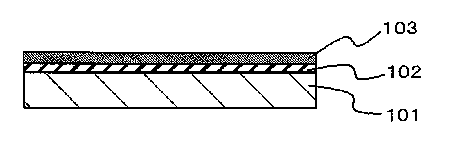
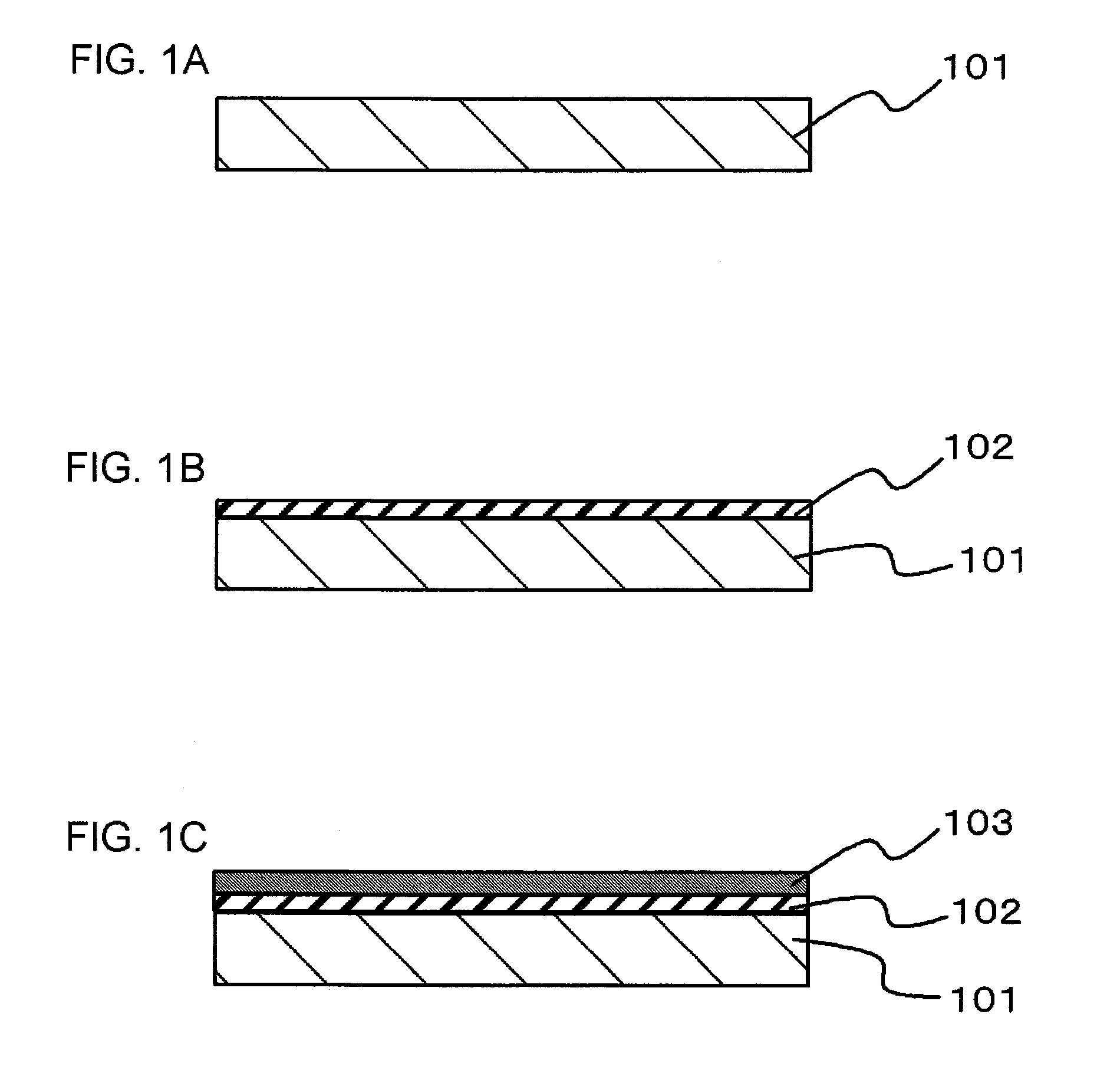
[0041]FIGS. 1A to 1C are diagrams for explaining a method of manufacturing a semiconductor device according to an embodiment. FIGS. 1A to 1C are simplified diagrams for the purpose of clearly explaining the invention, that is, the relationship between an underlying film 101, a first insulating film 102, and a second insulating film 103, and an interconnection layer (not shown), a barrier film (not shown), a cap film (not shown) and the like existing in an actual semiconductor manufacturing process. The embodiment includes forming the first insulating film 102 on the underlying film 101 by plasma polymerization of cyclic siloxane (FIG. 1B), and forming the second insulating film 103 on the first insulating film 102 by plasma polymerization of cyclic siloxane continuously after forming the first insulating film 102 (FIG. 1C). Here, the term “continuously” includes performing continuously to form the second insulating film 103 while a vacuum state is maintained after forming the first ...

second embodiment

[0067]The embodiment is also a method of manufacturing the semiconductor device. In the embodiment, only the points which are different from those of the first embodiment will be described, and identical contents will not be repeated. Even in the embodiment, as shown in FIGS. 1A to 1C, the first insulating film 102 is formed on the underlying film 101 by plasma polymerization of the cyclic siloxane, and the second insulating film 103 is continuously formed on the first insulating film 102 by plasma polymerization of the cyclic siloxane. In this manner, a laminated structure of the first insulating film and the second insulating film is formed. In the first embodiment, the film deposition rate is controlled by the RF power. However, in the embodiment, the ratio (a2 / (b2+c2)) of the gas flow rate (a2) of the cyclic siloxane to the sum (b2+c2) of the flow rate (b2) of the carrier gas and the flow rate (c2) of the excitation gas at forming the second insulating film 103 (FIG. 1C) is set ...

third embodiment

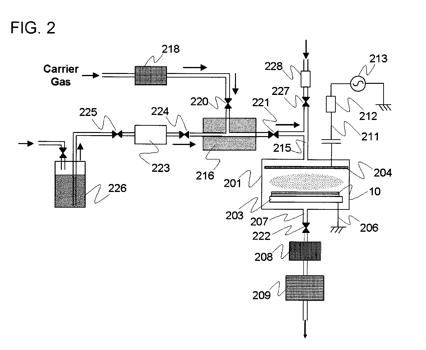
[0074]In the embodiment, only the points different from those of the first and second embodiments will be described, and identical contents will not be repeated. In the embodiment, when any of the first insulating film 102 and the second insulating film 103 is / are formed, an oxidized gas is supplied to the chamber 201 shown in FIG. 2 together with organosiloxane. In the embodiment, the carrier gas and the excitation gas can be used together with the cyclic siloxane gas and the oxidized gas. Oxygen (O2), carbon dioxide (CO2), nitrogen monoxide (N2O) and nitrogen dioxide (NO2) and the like can be used in the oxidized gas.

[0075]The film deposition rate can be improved by addition of the oxidized gas as shown in FIG. 15. Thereby, merits of the improvement in throughput and the reduction in the amount of the precursors used are generated, and thus an additional effect of the reduction in price can be expected.

[0076]The manufacturing method according to the embodiment is shown by a timing...


PUM


Abstract

A method of manufacturing a semiconductor device includes forming a first insulating film over an underlying film by plasma polymerization of cyclic siloxane, and forming a second insulating film on the first insulating film by plasma polymerization of the cyclic siloxane continuously, after forming the first insulating film. The deposition rate of the first insulating film is slower than the deposition rate of the second insulating film.

Description

[0001]This application is based on Japanese patent application Nos. 2010-004539 and 2010-129633, the content of which is incorporated hereinto by reference.BACKGROUND[0002]1. Technical Field[0003]The present invention relates to a method of manufacturing a semiconductor device.[0004]2. Related Art[0005]In recent years, as the miniaturization of semiconductors has progressed, there have been problems relating to an interconnection delay due to parasitic capacitance as well as to an increase in power consumption. For the purpose of avoiding these, low-dielectric constants of insulating films are being advanced.[0006]WO 2008 / 078649 discloses a barrier insulating film formed by plasma polymerization of cyclic siloxane including unsaturated hydrocarbon and amorphous carbon. This barrier insulating film has copper diffusion resistance, and the relative dielectric constant thereof is less than 3.5. For this reason, copper-containing interconnections are coated with this barrier insulating ...

Claims


Application Information

Patent Timeline
Patent Type & Authority Applications(United States)
IPC IPC(8): H01L51/40
CPCH01L21/02126H01L21/022H01L21/02203H01L21/76883H01L21/76826H01L21/76829H01L21/76832H01L21/02274
Inventor YAMAMOTO, HIRONORIHAYASHI, YOSHIHIROKAWAHARA, JUNUSAMI, TATSUYAOHTO, KOICHI
Owner RENESAS ELECTRONICS CORP
Why Eureka
Try Eureka