Method of manufacturing semiconductor device

a manufacturing method and technology of semiconductors, applied in the direction of semiconductor devices, basic electric elements, electrical equipment, etc., can solve the problems of abnormal electrical discharge in the initial stage of film deposition, increase in power consumption, and deterioration of the thickness uniformity of the entire insulating film, so as to reduce detachment and the like, without deteriorating the reliability of the device, and achieve the effect of reducing the number of detachable parts

Inactive Publication Date: 2013-05-07
RENESAS ELECTRONICS CORP
View PDF15 Cites 1 Cited by
  • Summary
  • Abstract
  • Description
  • Claims
  • Application Information

AI Technical Summary

Benefits of technology

[0013]According to the invention, when the insulating film is formed on the underlying film by plasma polymerization of organosiloxane having a Si—O cyclic structure, the deposition rate of the first insulating film at the beginning of film deposition is made slower than the deposition rate of the second insulating film at the late stage of film deposition. Thereby, since a change in impedance of the film deposition surface in the initial stage of film deposition can be caused to be slow, plasma is stabilized, and thus the generation of an abnormal electrical discharge in the initial stage of film deposition can be suppressed. Therefore, it is possible to form an insulating film having a lower relative dielectric constant without deteriorating reliability of the device. At the same time, the adhesion strength to the underlying layer is raised, and detaching and the like is reduced, so that process resistance of chemical mechanical polishing (CMP) and the like or mounting resistance is improved.
[0014]According to the invention, it is possible to form the insulating film having a lower relative dielectric constant without deteriorating reliability of the device.

Problems solved by technology

In recent years, as the miniaturization of semiconductors has progressed, there have been problems relating to an interconnection delay due to parasitic capacitance as well as to an increase in power consumption.
However, the inventors has been found that when plasma polymerization is performed in which cyclic siloxane disclosed in WO 2008 / 078649 pamphlet is used, there exist the film deposition conditions which cause an abnormal electrical discharge in the initial stage of film deposition.
For this reason, there may be a case where the thickness of the insulating film in the initial stage of film deposition becomes nonuniform, and the thickness uniformity of the entire insulating film is deteriorated.
In addition, when the insulating film is formed on a transistor, there may also be a case where damage is given to a gate insulating film due to this abnormal electrical discharge.

Method used


Image

  • Method of manufacturing semiconductor device
  • Method of manufacturing semiconductor device
  • Method of manufacturing semiconductor device

Examples


example 1

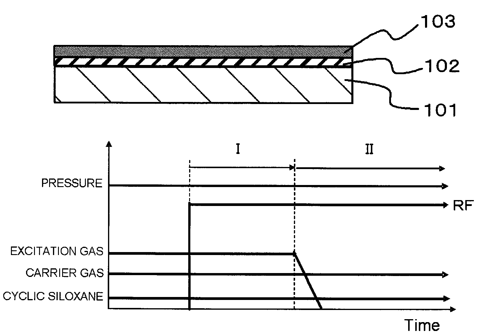
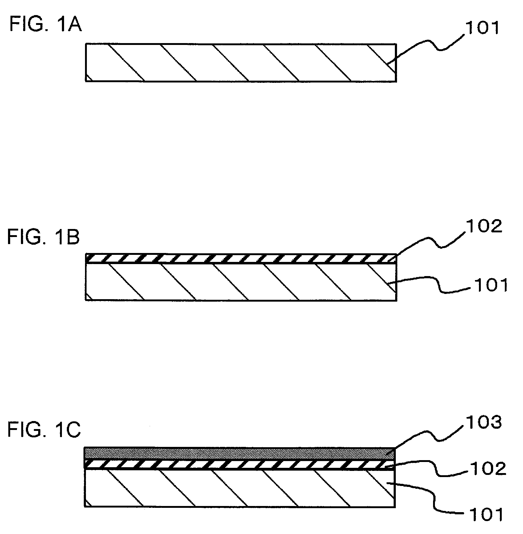
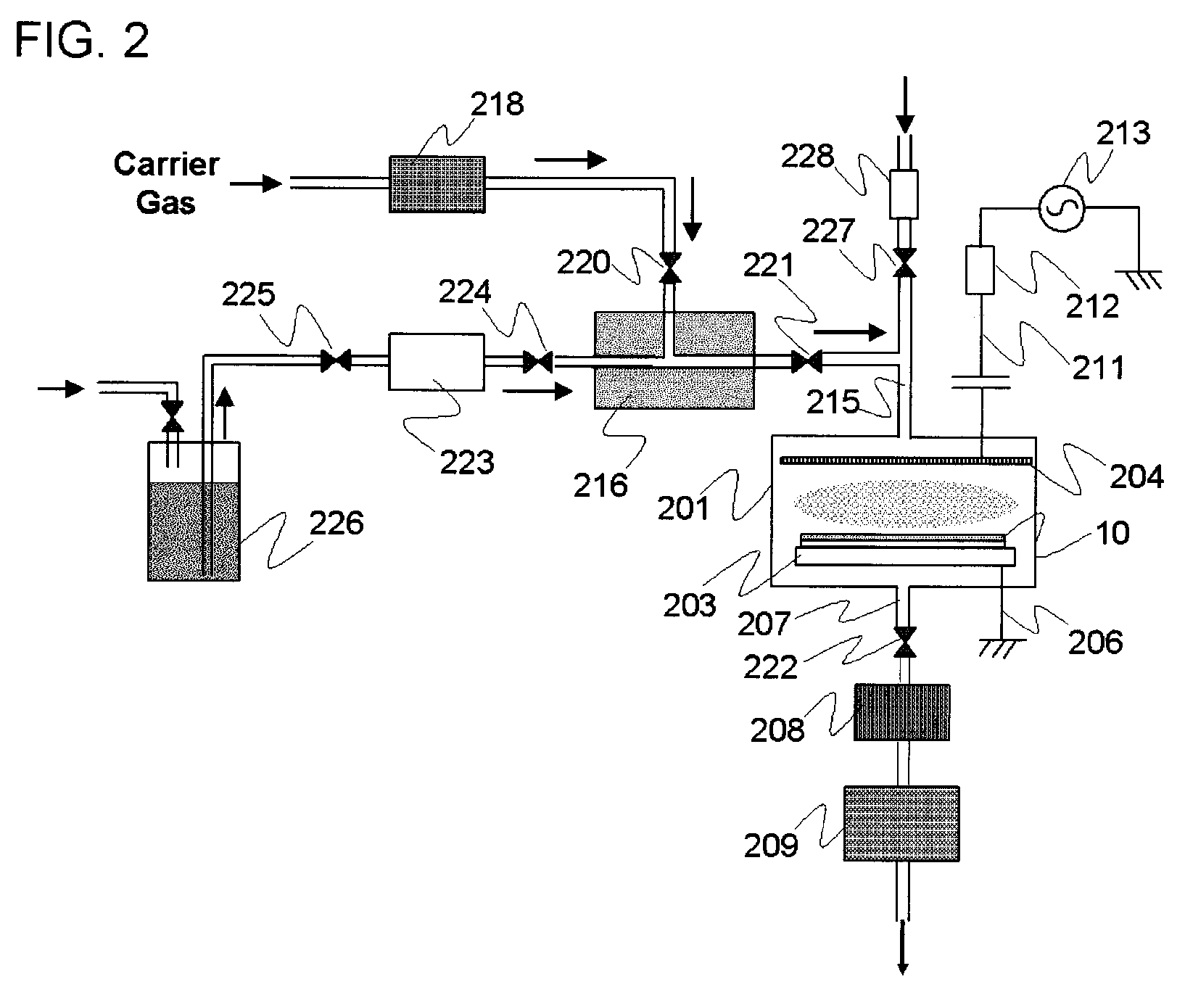
[0107]The first insulating film 102 and the second insulating film 103 were formed according to the timing diagram of FIG. 3 using the configuration shown in FIGS. 1A to 1C. As the plasma generation apparatus, an apparatus shown in FIG. 2 was used. In the example, a silicon substrate was used as the underlying film 101 in order to perform the measurement of the film thickness uniformity more simply. Trivinyltriisopropylcyclotrisiloxane represented by the above-mentioned Formula (11) was used as the cyclic siloxane, and a He gas was used as the carrier gas. The pressure within the chamber was maintained at 280 Pa. In I region of FIG. 3, the RF power was controlled so as to have a film deposition rate of 90 nm / minute, and the first insulating film 102 was formed to have a thickness of 10 nm. At this time, in the in-plane distribution measurement of the film thickness uniformity in which a spectroscopic ellipsometer was used, the in-plane uniformity of thickness of the first insulating...

example 2

[0112]In the method of Example 1, whether the abnormal electrical discharge had arisen or not was examined by changing the thicknesses of the first insulating film 102 to be formed at 0, 3, 7, 8, 10, and 15 nm, respectively. The result is shown in Table 1.

[0113]

TABLE 1Thickness of FirstHad Abnormal ElectricalInsulating FilmDischarge Arisen?0 nmYes3 nmYes7 nmYes8 nmYes10 nm No15 nm No

[0114]When the first insulating film 102 was formed at less than 10 nm, the abnormal electrical discharge was confirmed in the initial stage of formation of the second insulating film 103. On the other hand, when the first insulating film 102 was formed to have a thickness of 10 nm and 15 nm, the abnormal electrical discharge was not confirmed throughout forming the first and second insulating films 102 and 103.

example 3

[0115]An antenna test element group (TEG) wafer was used in which a gate electrode having a pad was created on a MOS capacitor in order to measure plasma damage at the time of formation. An antenna ratio is defined as a ratio of the gate electrode area to the gate area. The wafer size is 300 mm, and the thickness of the gate insulating film is 2 nm. The first and second insulating films 102 and 103 were sequentially formed according to the timing diagram of FIG. 3 using this TEG wafer as the underlying film 101 of FIGS. 1A to 1C. Trivinyltriisopropylcyclotrisiloxane represented by the above-mentioned Formula (11) was used as the cyclic siloxane, and a helium gas was used as the carrier gas. In I region of FIG. 3, the RF power was controlled so as to have a film deposition rate of 90 nm / minute, and the first insulating film 102 having a thickness of 10 nm was formed. Thereafter, the film deposition rate was set to 120 nm / minute for ten seconds, and the second insulating film 103 havi...


PUM


Abstract

A method of manufacturing a semiconductor device includes forming a first insulating film over an underlying film by plasma polymerization of cyclic siloxane, and forming a second insulating film on the first insulating film by plasma polymerization of the cyclic siloxane continuously, after forming the first insulating film. The deposition rate of the first insulating film is slower than the deposition rate of the second insulating film.

Description

[0001]This application is based on Japanese patent application Nos. 2010-004539 and 2010-129633, the content of which is incorporated hereinto by reference.BACKGROUND[0002]1. Technical Field[0003]The present invention relates to a method of manufacturing a semiconductor device.[0004]2. Related Art[0005]In recent years, as the miniaturization of semiconductors has progressed, there have been problems relating to an interconnection delay due to parasitic capacitance as well as to an increase in power consumption. For the purpose of avoiding these, low-dielectric constants of insulating films are being advanced.[0006]WO 2008 / 078649 discloses a barrier insulating film formed by plasma polymerization of cyclic siloxane including unsaturated hydrocarbon and amorphous carbon. This barrier insulating film has copper diffusion resistance, and the relative dielectric constant thereof is less than 3.5. For this reason, copper-containing interconnections are coated with this barrier insulating ...

Claims


Application Information

Patent Timeline
Patent Type & Authority Patents(United States)
IPC IPC(8): H01L51/40
CPCH01L21/02126H01L21/022H01L21/02203H01L21/02274H01L21/76826H01L21/76829H01L21/76832H01L21/76883
Inventor YAMAMOTO, HIRONORIHAYASHI, YOSHIHIROKAWAHARA, JUNUSAMI, TATSUYAOHTO, KOICHI
Owner RENESAS ELECTRONICS CORP
Why Eureka
Try Eureka