Photovoltaic device having transparent electrode formed with nanoparticles

a photovoltaic device and nanoparticle technology, applied in thermoelectric devices, electrically conductive paints, transportation and packaging, etc., can solve the problems of inferior transparency, marginal conductivity, and a large number of ito films

Inactive Publication Date: 2011-07-21
CIMA NANOTECH ISRAEL
View PDF13 Cites 36 Cited by
  • Summary
  • Abstract
  • Description
  • Claims
  • Application Information

AI Technical Summary

Benefits of technology

[0008]The present inventions seeks to provide an improved method for producing devices for converting light to electricity and improved devices produced thereby.
[0009]The method and device include a transparent electrode comprising a pattern of conductive traces formed of at least partially joined nanoparticles defining randomly-shaped cells generally free of nanoparticles and generally transparent to light. The conductive traces self-assemble from a liquid emulsion containing the nanoparticles after the emulsion is coated onto a substrate and dried. The traces can be formed on the substrate by conventional liquid coating processes that do not require physical contact of the coating equipment with the substrates thereby reducing the possibility of breakage to the substrate. The electrode is flexible and can be made by cost-effective roll-to-roll coating processes.

Problems solved by technology

ITO films suffer from a number of disadvantages including inferior transparency, particularly in the infrared and ultraviolet regions of the spectrum, and marginal conductivity.
Both of these disadvantages result in lower efficiency of the solar cell.
ITO is also expensive and concerns have been raised about dwindling global supplies of indium.
ITO is also brittle and does not lend itself to roll-to-roll processing or use in flexible solar cells.
Silver wire grids also have significant drawbacks, especially in the fabrication of solar cells with silicon wafers.
The application of the grid pattern to the silicon wafer by contact printing techniques can result in significant wafer breakage.
Sensitivity to breakage requires manufacturers to use thicker silicon substrates than might otherwise be preferred, and the thickness of silicon substrates is a dominant factor in overall cell cost.
Further, conventional screen printed Ag electrodes tend to have poor geometries, including poor aspect ratios for front electrode purposes, meaning they are relatively wide (casting a large shadow) and relatively short (meaning offering less overall electrical conductance than would be preferred).
Further, they cannot be printed in close proximity to each other owing to resolution limits.

Method used


Image

  • Photovoltaic device having transparent electrode formed with nanoparticles
  • Photovoltaic device having transparent electrode formed with nanoparticles
  • Photovoltaic device having transparent electrode formed with nanoparticles

Examples


Embodiment Construction

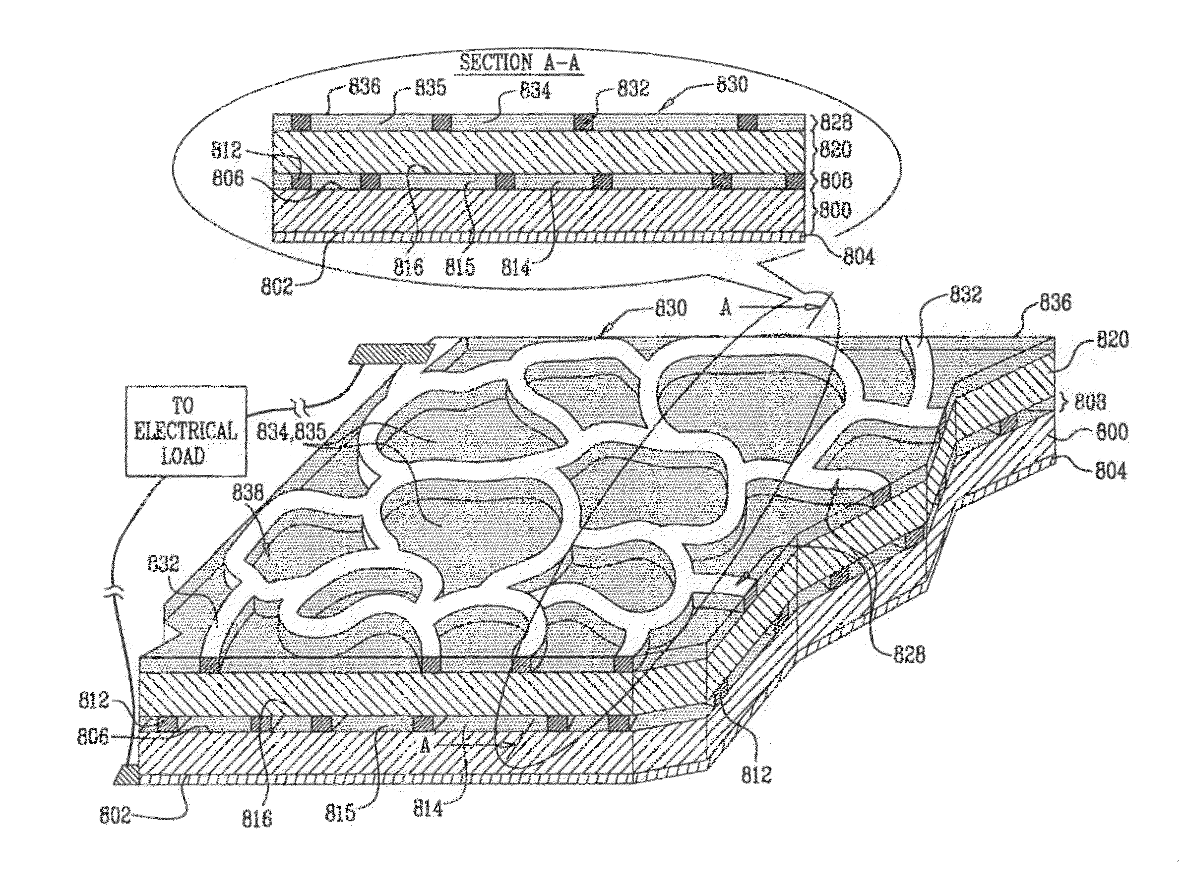
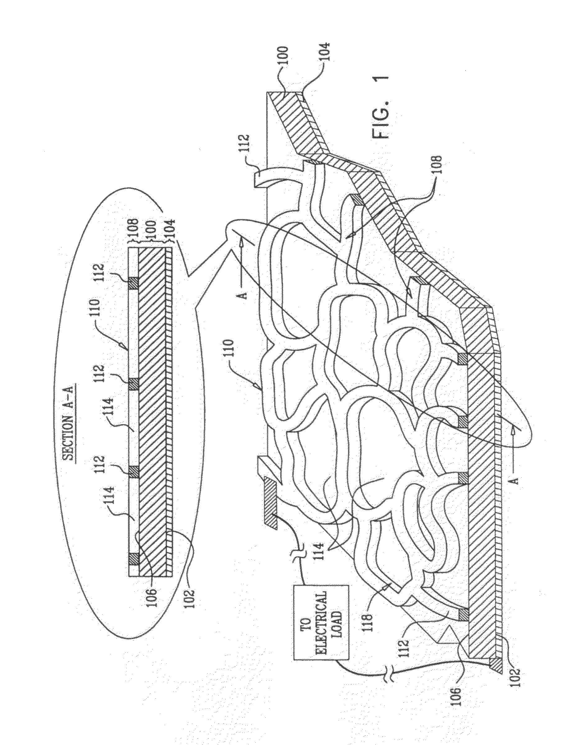
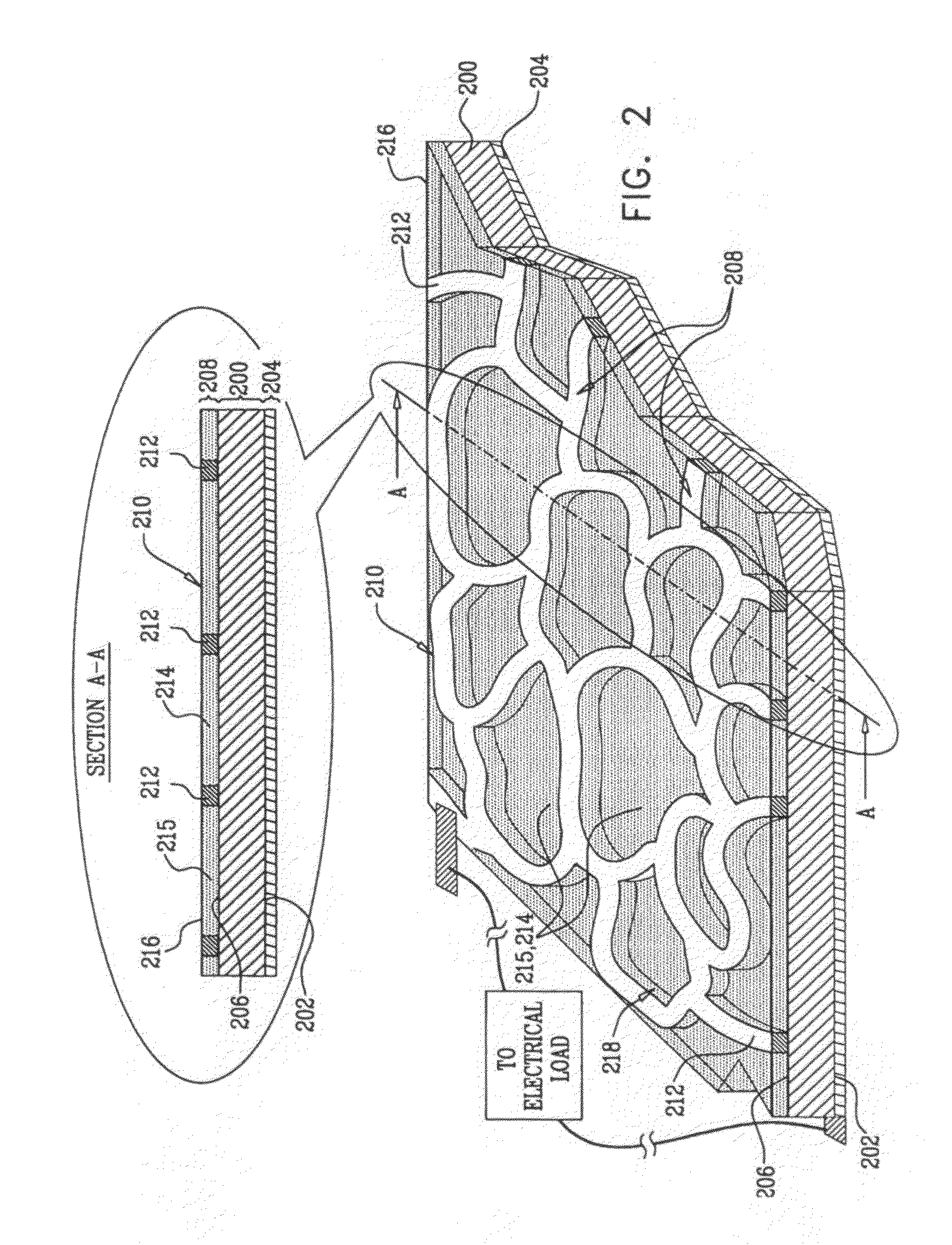
[0038]Reference is now made to FIG. 1, which is a simplified illustration of a device for converting light to electricity in accordance with a one embodiment of the present invention.

[0039]As seen in FIG. 1, the device for converting light to electricity comprises a semiconductor substrate 100 having formed on an underside surface 102 thereof and in effective electrical contact therewith, an electrode 104.

[0040]The semiconductor substrate 100 may be any suitable semiconductor substrate, for example, materials known in the art as inorganic semiconductors, including but not limited to, silicon, geranium, compounds of boron, tellurium, gallium, or tin, and compounds such as gallium arsenide (GaAs), gallium phosphide (GaP), indium phosphide (InP), cadmium telluride (CdTe), cadmium sulphide (CdS), gallium aluminum arsenide (GaAlAs), mercury cadmium telluride (HgCdTe), gallium arsenide phosphide (GaAsP), copper indium gallium diselenide (CIGS), and copper indium selenide or sulfide.

[0041]...


PUM

PropertyMeasurementUnit
diametersaaaaaaaaaa
thicknessaaaaaaaaaa
thicknessaaaaaaaaaa

Abstract

A photovoltaic device is disclosed that includes a transparent front electrode formed by the self-assembly of conductive nanoparticles from an emulsion coated onto a substrate and dried. The nanoparticles self-assemble into a network-like pattern of conductive traces that define randomly-shaped transparent cells. The cells may be filled with various transparent filler materials and additional layers may be present in the device in addition to conventional components. Processes for forming the transparent electrode are also disclosed.

Description

FIELD OF THE INVENTION[0001]The present invention relates to a method for producing devices for converting light to electricity and devices produced thereby.BACKGROUND OF THE INVENTION[0002]The photovoltaic effect used in solar cells allows direct conversion of light energy from the sun's rays into electricity by way of the generation and transport inside a semiconductor material of positive and negative electrical charges. The action of light impinging on the semiconductor material creates positive and negative charges unbound, or weakly bound, to each other, that are capable of diffusing to or being otherwise captured by different electrodes in contact with the semiconductor.[0003]Electrodes are placed on both sides of the semiconductor material to collect the electrical charge. Light must enter the solar cell through at least one of the electrodes, generally referred to as the “front” electrode. Thus, the front electrode must be transparent to light as well as be electrically con...

Claims


Application Information

Patent Timeline
Patent Type & Authority Applications(United States)
IPC IPC(8): H01L51/46H01L51/48
CPCH01L31/1884Y10T428/24876H01L33/42H01L51/445Y02E10/50H01B1/22H01B1/20H01B1/24B32B15/02H05B33/26H01L2924/0002H01L33/38Y10T428/24893Y10T156/10H01L2924/00H10K30/83B05D5/12C09D5/24
Inventor DE LA VEGA, FERNANDOMOIRA, NIR M.GARBAR, ARKADY
Owner CIMA NANOTECH ISRAEL
Why Eureka
Try Eureka