

Light Emitting Element and Light Emitting Device
a technology of light emitting elements and light emitting devices, which is applied in the direction of thermoelectric devices, glass/slag layered products, chemistry apparatuses and processes, etc., can solve the problems of poor color conversion efficiency of blue to red in principle, unnecessary back light used for the conventional liquid crystal display device, and deterioration of contrast, etc., to achieve high light emission efficiency and high efficient light emission
- Summary
- Abstract
- Description
- Claims
- Application Information
AI Technical Summary
Benefits of technology
Problems solved by technology
Method used
Image

Examples
example 1
[0086]In this example, a device configuration of a light emitting element and a method for manufacturing thereof according to the present invention will be explained with reference to FIG. 5.
[0087]An anode 501 of the light emitting element is formed over a glass substrate 500 having an insulating surface. As a material for the anode 501, ITO, a transparent conductive film, is used. The anode 501 is formed by sputtering to have a thickness of 110 nm. The anode 501 is square in shape and 2 mm in height and width.
[0088]Then, an electroluminescent layer 502 is formed over the anode 501. In this example, the electroluminescent layer 502 has a lamination structure comprising a hole injecting layer 511; a first light emitting layer 512, which has hole injection properties; a second light emitting layer 513; an electron transporting layer 514; and an electron injecting layer 515. The first light emitting layer 512 is formed by a material, which can achieve blue emission, specifically, a mat...
example 2
[0097]In this example, device characteristics of the light emitting element described in Example 1 having the configuration: ITO / Cu-Pc (20 nm) / α-NPD (30 nm) / CBP+Pt(ppy)acac: 15 wt % (20 nm) / BCP (30 nm) / CaF (2 nm) / Al (100 nm) will be explained. Emission spectrum of the light emitting element having the above described configuration is shown by each spectrum 1 in FIG. 8 and FIG. 9. Each plot 1 in FIGS. 10 to 13 shows for electric characteristics.
[0098]Spectrum 1 in FIG. 8 shows the emission spectrum of the light emitting element having the above described configuration at an applied current of 1 mA (approximately 960 cd / m2). From the result shown by spectrum 1, white emission can be obtained having three components: blue emission from α-NPD composing the first light emitting layer (˜450 nm); green emission of phosphorescent light emission from Pt(ppy)acac contained in a second light emitting layer (˜490 nm, ˜530 nm); and orange emission from excimer light emission of Pt(ppy)acac conta...
example 3
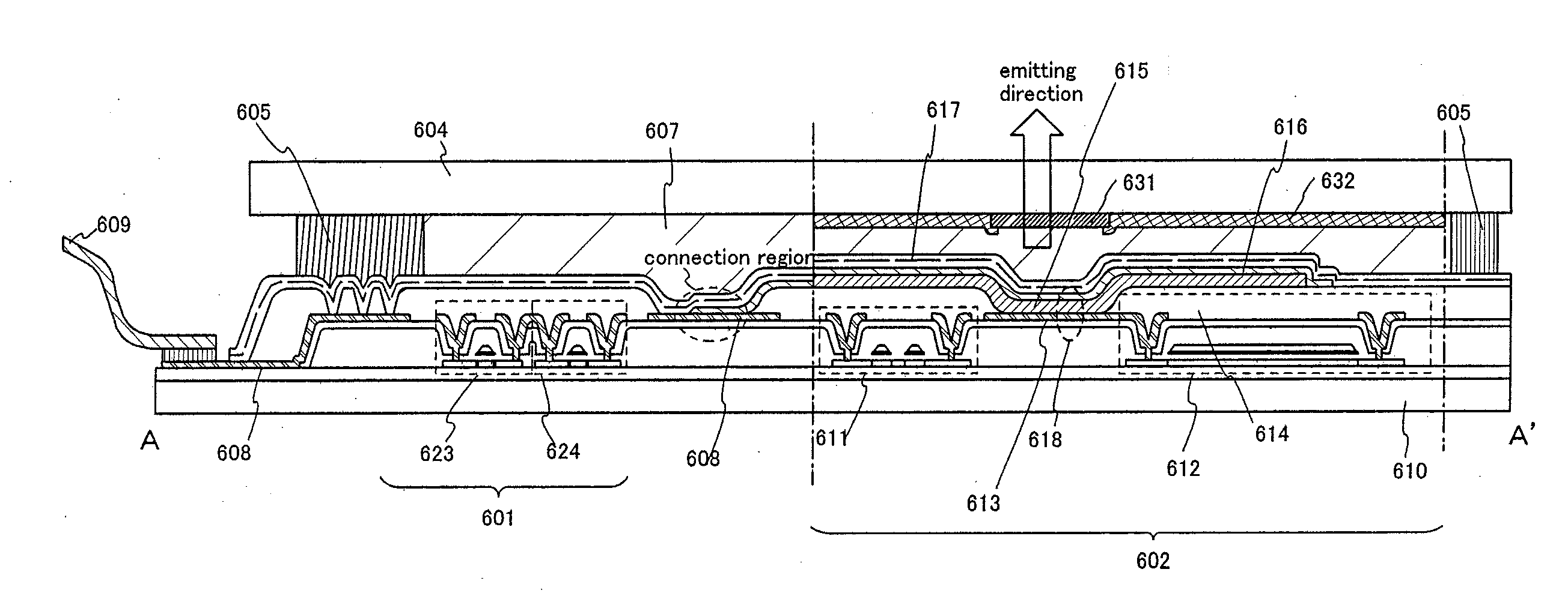
[0113]In this example, a method for manufacturing a light emitting device (top emission structure) having a light emitting element according to the present invention, which exhibits white emission, over a substrate having an insulating surface will be explained with reference to FIG. 6. As used herein, the term “top emission structure” refers to a structure in which light is extracted from the opposite side of the substrate having an insulating surface.
[0114]FIG. 6A is a top view of a light emitting device. FIG. 6B is a cross-sectional view of FIG. 6A taken along the line A-A′. Reference numeral 601 indicated by a dotted line denotes a source signal line driver circuit; 602, a pixel portion; 603, a gate signal line driver circuit; 604, a transparent sealing substrate; 605, a first sealing agent; and 607, a second sealing agent. The inside surrounded by the first sealing agent 605 is filled with the transparent second sealing agent 607. In addition, the first sealing agent 605 contai...
PUM
| Property | Measurement | Unit |
|---|---|---|
| wavelength region | aaaaa | aaaaa |
| wavelength region | aaaaa | aaaaa |
| wavelength | aaaaa | aaaaa |
Abstract
Description
Claims
Application Information