Semiconductor memory device, driving method thereof, and method for manufacturing semiconductor device

a semiconductor memory and semiconductor technology, applied in the field of memory devices, can solve the problems of not meeting all necessary conditions of semiconductor devices, the size of a power supply device needs to be larger, and the device has good and bad points, so as to achieve the effect of small variation in the amount of charge at the time of writing data and reducing the threshold value of the whole semiconductor memory devi

Inactive Publication Date: 2011-08-25
SEMICON ENERGY LAB CO LTD
View PDF99 Cites 31 Cited by
  • Summary
  • Abstract
  • Description
  • Claims
  • Application Information

AI Technical Summary

Benefits of technology

[0050]In the case where the charge is reduced due to the leakage current, refreshing may be performed similarly to a conventional DRAM; an interval between refreshing operations is determined depending on a period during which the charge can be held. In the case where the charge is held for such a long period as described above, refreshing is necessary, for example, only once a month or once a year. Frequent refreshing which is needed in a conventional DRAM is not necessary and thus power consumption of a semiconductor memory device is reduced.
[0051]Note that in a conventional DRAM, operation of writing data is needed again every time when the data is read; on the other hand, in a semiconductor memory device according to an embodiment of the present invention, such operation is unnecessary because data is not lost by operation of reading the data. Such a feature could be realized only in an SRAM; however, in the semiconductor memory device according to an embodiment of the present invention, the number of transistors used in one memory cell is five or less, typically 2, which is smaller than that in the case of a conventional SRAM. Furthermore, when one of the transistors is formed using an oxide semiconductor in a thin film shape, an increased integration degree can be obtained because the transistor can be stacked over a conventional silicon semiconductor.
[0058]In order to further increase such an effect of the present invention, an S value of a transistor used may be grater than or equal to 59 mV / dec and less than or equal to 70 mV / dec, preferably greater than or equal to 59 mV / dec and less than or equal to 63 mV / dec at a temperature when the transistor is in use. In this manner, a variation in threshold values in the whole semiconductor memory device can be reduced, which is a matter of course. In particular, when the writing transistor has an S value in the above range, a variation in the amount of charge at the time of writing data becomes small. In addition, when the reading transistor has an S value in the above range, the potential to be applied to the reading word line at the time of reading can be set with a short interval. These features are advantageous in the case of dealing with multivalued data in a semiconductor memory device.

Problems solved by technology

As described above, a conventional semiconductor memory device has good points and bad points and there has been no semiconductor devices meeting all necessary conditions.
When the power consumption is high, the size of a device for supplying power needs to be larger, or an operating time on a battery is shortened.
Moreover, a semiconductor element may be heated; thus, the characteristics of the element may be deteriorated, and in some cases, a circuit is damaged.
In light of these points, a DRAM has difficulty in reducing power consumption because leakage current is generated and refreshing is performed all the time.
In contrast, in an SRAM, although a problem of power consumption can be solved to some extent, there is another problem in that the integration degree cannot be increased because six transistors are included in one memory cell.

Method used


Image

  • Semiconductor memory device, driving method thereof, and method for manufacturing semiconductor device
  • Semiconductor memory device, driving method thereof, and method for manufacturing semiconductor device
  • Semiconductor memory device, driving method thereof, and method for manufacturing semiconductor device

Examples


embodiment 1

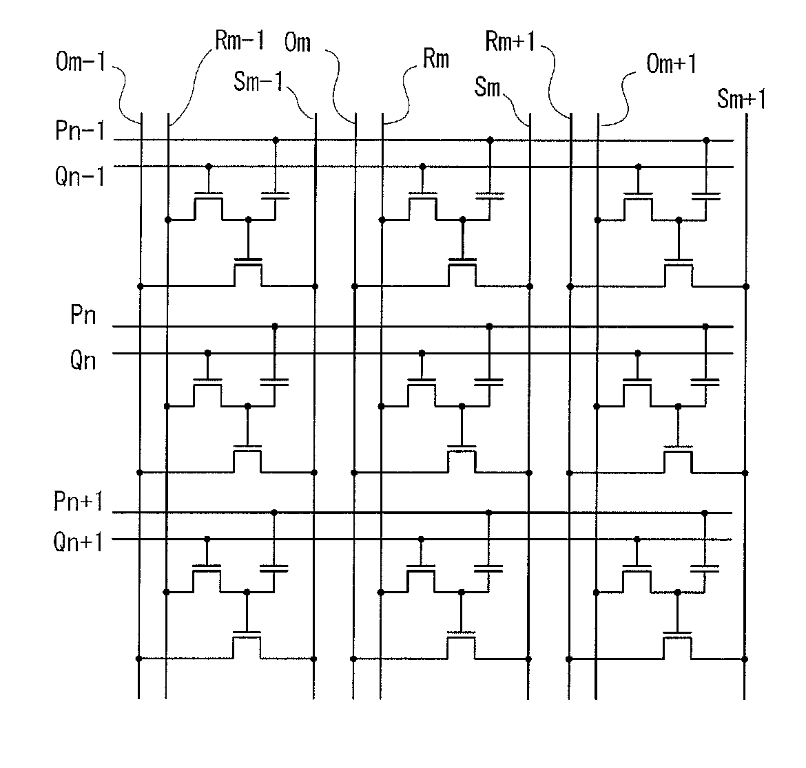
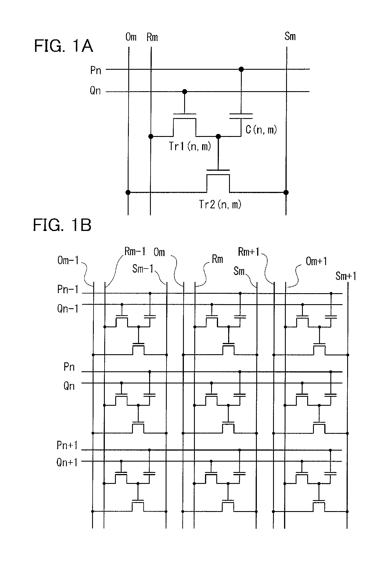
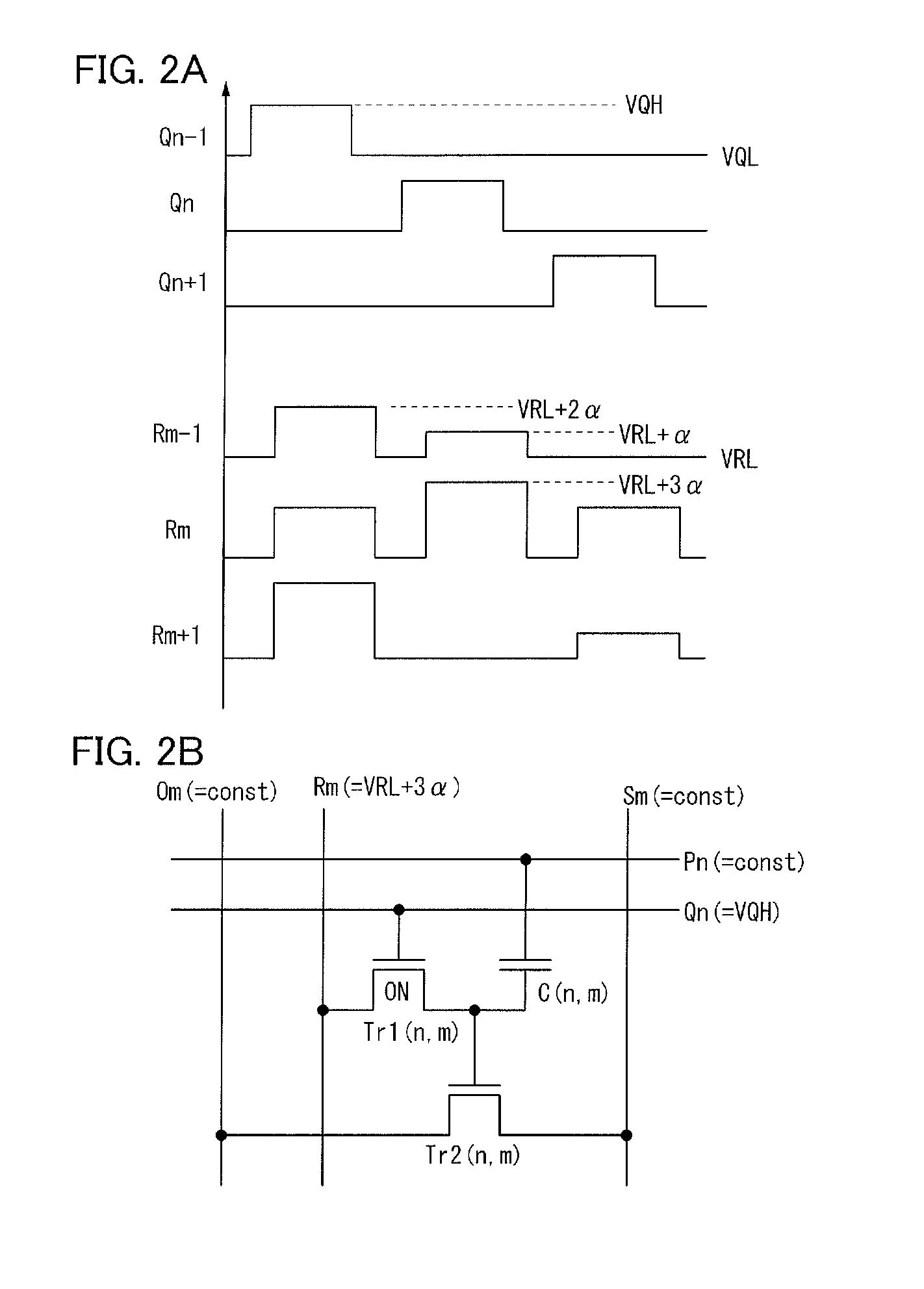
[0077]In this embodiment, operation of a semiconductor memory circuit illustrated in FIGS. 1A and 1B is described. Here, both the writing transistor Tr1 and the reading transistor Tr2 are n-channel transistors. First, a writing method is described with reference to FIGS. 2A and 2B. At the time of writing, the reading bit lines ( . . . , Om−1, Om, Om+1, . . . ), the bias lines ( . . . , Sm−1, Sm, Sm+1, . . . ), and the reading word lines Pn−1, Pn, Pn+1, . . . ) are held at constant potential. Although potential may be different depending on the kind of a wiring, the potential of any wiring is set to 0 volt here.

[0078]In this state, a pulse is sequentially applied to the writing word lines ( . . . , Qn−1, Qn, Qn+1, . . . ) so that the writing transistor is turned on / off. Here, the potential of the writing word line when the pulse is not applied is VQL and potential of the pulse is VQH. As illustrated in FIG. 2A, by sequentially applying the pulse in each row, the writing transistor is...

embodiment 2

[0092]In this embodiment, operation of a semiconductor memory circuit illustrated in FIGS. 5A and 5B is described. Here, both the writing transistor Tr1 and the reading transistor Tr2 are n-channel transistors. In this embodiment, the writing bit line in Embodiment 1 is substituted for the reading bit line. As described above, by employing this structure, the number of wirings of a semiconductor memory device can be smaller than that in Embodiment 1.

[0093]A writing method is almost the same as the writing method in Embodiment 1. The bias lines ( . . . , Sm−1, Sm, Sm+1, . . . ) and the reading word lines ( . . . , Pn−1, Pn, Pn+1, . . . ) are held at constant potential. Although potential may be different depending on the kind of a wiring, the potential of any wiring is set to 0 volt here.

[0094]Then, a pulse is sequentially applied to the writing word lines ( . . . , Qn−1, Qn, Qn+1, . . . ) as illustrated in FIG. 2A so that the writing transistor is turned on / off. At the same time, a ...

embodiment 3

[0099]In this embodiment, a shape and a manufacturing method of the semiconductor memory device described in Embodiment 2 are described. In this embodiment, an oxide semiconductor containing zinc and indium is used for the writing transistor Tr1 and a single crystal silicon semiconductor is used for the reading transistor Tr2. Therefore, the writing transistor Tr1 is stacked over the reading transistor Tr2.

[0100]That is, an insulated gate transistor using a single crystal silicon semiconductor which is provided over a single crystal silicon substrate is used as the reading transistor Tr2 and a transistor in which an oxide semiconductor is used for a semiconductor layer is formed thereover as the writing transistor Tr1. Note that although an example in which a semiconductor memory device is formed over a single crystal silicon substrate is described in this embodiment, the semiconductor memory device can be provided over another kind of semiconductor substrate or an insulating substr...


PUM


Abstract

A matrix is formed using a plurality of memory cells in each of which a drain of the writing transistor is connected to a gate of a reading transistor and one electrode of a capacitor. A gate of the writing transistor, a source of the writing transistor, a source of the reading transistor, and a drain of the reading transistor are connected to a writing word line, a writing bit line, a reading bit line, and a bias line, respectively. The other electrode of the capacitor is connected to a reading word line. In order to decrease the number of wirings, the writing bit line is substituted for the reading bit line. The reading bit line is formed so as to be embedded in a groove-like opening formed over a substrate.

Description

TECHNICAL FIELD[0001]The present invention relates to a memory device using a semiconductor.BACKGROUND ART[0002]There are many kinds of memory devices using semiconductors. For example, a dynamic random access memory (DRAM), a static random access memory (SRAM), an electrically erasable and programmable read only memory (EEPROM), a flash memory, and the like can be given.[0003]In a DRAM, data is stored by holding charge in a capacitor which is provided in a memory cell. However, even when a transistor used for switching is in an off state, a slight amount of leakage current is generated between a source and a drain; thus, the data is lost within a relatively short time (several tens of seconds at the longest). Therefore, the data needs to be rewritten (refreshed) in a certain cycle (generally several tens of milliseconds).[0004]In an SRAM, data is held by utilizing a bistable state of a flip-flop circuit. Although a CMOS inverter is generally used in a flip-flop circuit of an SRAM, ...

Claims


Application Information

Patent Timeline
Patent Type & Authority Applications(United States)
IPC IPC(8): G11C5/10G11C11/40H01L21/336H01L29/94
CPCG11C16/0408H01L27/0629H01L27/115H01L27/1225H01L27/11521H01L27/1156H01L27/11519H10B41/10H10B41/70H10B69/00H10B41/30H01L29/78645
Inventor TAKEMURA, YASUHIKO
Owner SEMICON ENERGY LAB CO LTD
Why Eureka
Try Eureka