Organic electroluminescent element and display device
a technology of electroluminescent elements and display devices, which is applied in the direction of organic semiconductor devices, thermoelectric devices, solid-state devices, etc., can solve the problems of drive voltage reduction, achieve the effect of reducing the resistance of the n-doped layer during charge transfer, facilitating charge transfer, and efficient transfer
- Summary
- Abstract
- Description
- Claims
- Application Information
AI Technical Summary
Benefits of technology
Problems solved by technology
Method used
Image

Examples
first embodiment
1. First embodiment
(1-1) Organic electroluminescent element (example of top emission type)
(1-2) Display device (usage example of the organic electroluminescent element)
2. Second embodiment (wiring material)
1. First Embodiment
[(1-1) Organic Electroluminescent Element (Example of Top Emission Type)]
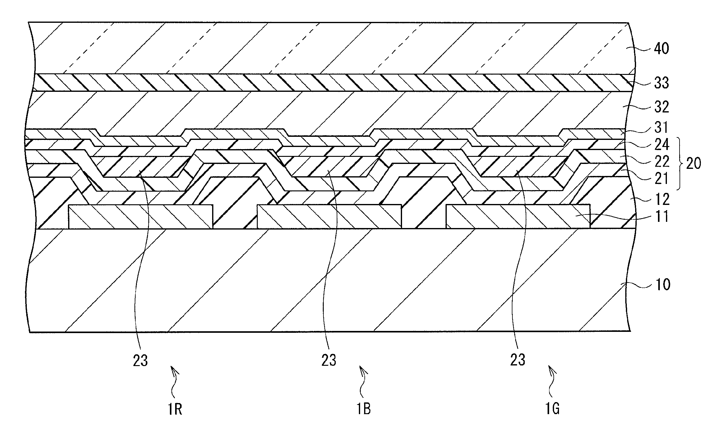
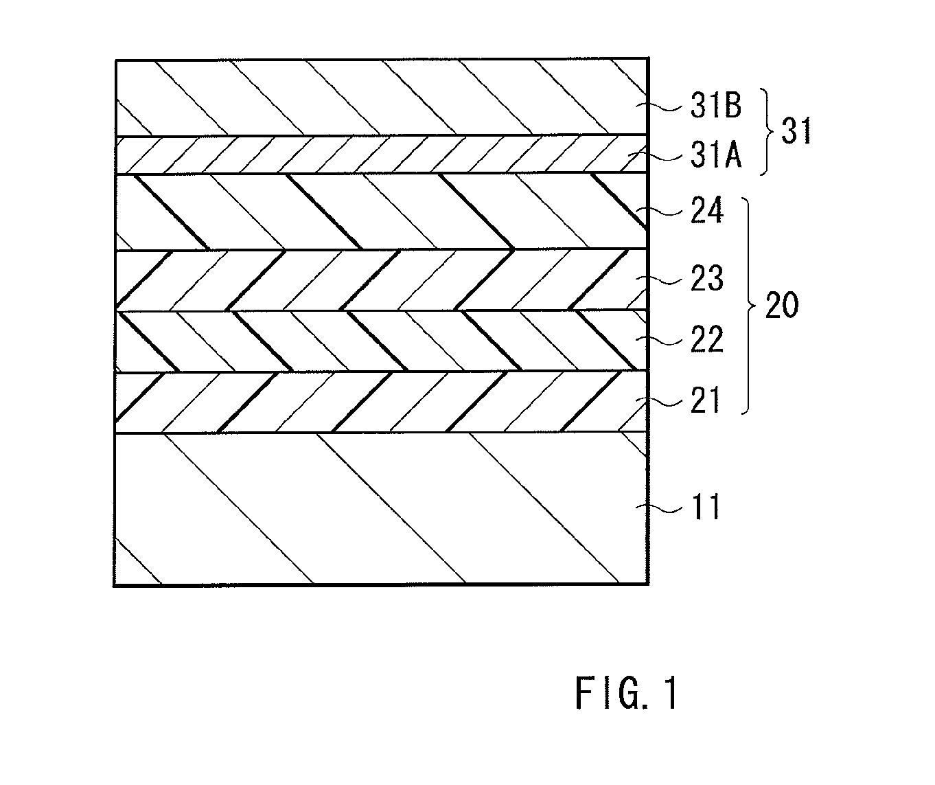
[0021]FIG. 1 shows a sectional configuration of an organic electroluminescent element according to a first embodiment of the invention. The organic electroluminescent element (organic EL element) is used for a display device such as a color display. The organic electroluminescent element has an organic layer 20 between an anode 11 and a cathode 31. The organic layer 20 has a structure where an n-doped layer 21, a hole transport layer 22, a light emitting layer 23 and an electron transport layer 24 are stacked in order from an anode 11 side. Here, description is made on a top-emission-type organic electroluminescent element where light emitted from the light emitting layer 23 (hereinafter, c...
second embodiment (
2. Second Embodiment (Wiring Material)
[0086]A wiring material according to a second embodiment of the invention is used for a circuit board mounted in a display device or the like, and is an n-doped, organic conductive material including the n-type host material and the n-type dopant material. According to this, current application may be performed at low voltage.
[0087]For example, the wiring material may be used for a wiring structure shown in FIG. 5. FIG. 5 schematically shows a wiring structure using the wiring material. The wiring structure has an n-doped layer 52 as a layer including the wiring material between a first electrode 51 (for example, anode) and a second electrode 53 (for example, cathode).
[0088]For example, the first electrode 51 has the same configuration as the anode 11 of the organic electroluminescent element. Moreover, the n-doped layer 52 is formed of a wiring material including the n-type host material and the n-type dopant material, and thus has the same con...
experimental example 1-6
[0094]A wiring structure was produced through the same procedure as in the experimental example 1-1 except that a layer including the compound (HAT) expressed by the formula (3-1) was formed in place of the n-doped layer 52 by vacuum evaporation with a thickness of 100 nm.
TABLE 1N-doped layerN-type dopantcompoundSecond electrodeFirstN-type hostDoping amountSecondelectrodecompoundType(percent by mass)First layerlayerExperimentalAlFormulaFormula0.5LiFMgAgexample 1-1(3-1)(2-1)ExperimentalHATαNPD1.0example 1-2Experimental2.0example 1-3Experimental4.0example 1-4Experimental10.0example 1-5ExperimentalAlFormula——LiFMgAgexample 1-6(3-1)HAT
[0095]A voltage up to 3 V was applied between the electrodes of each of the wiring structures of the experimental examples 1-1 to 1-6 so that current density was measured. As a result, results as shown in FIG. 6 were obtained.
[0096]As shown in FIG. 6, current density was extremely high in the experimental examples 1-1 to 1-5, in which the n-doped layer 52 ...
PUM
 Abstract
Description
Claims
Application Information
 - R&D
- Intellectual Property
- Life Sciences
- Materials
- Tech Scout
- Unparalleled Data Quality
- Higher Quality Content
- 60% Fewer Hallucinations
Browse by: Latest US Patents, China's latest patents, Technical Efficacy Thesaurus, Application Domain, Technology Topic, Popular Technical Reports.
© 2025 PatSnap. All rights reserved.Legal|Privacy policy|Modern Slavery Act Transparency Statement|Sitemap|About US| Contact US: help@patsnap.com