Active matrix organic electroluminescent device and method of manufacture thereof

a technology of organic electroluminescent devices and active matrix, which is applied in the direction of luminescent coating applications, discharge tubes luminescent screens, other domestic articles, etc., can solve the problems of easy falling off of the driving circuit of the organic electroluminescent device from the active matrix, difficult operation, and high cost, so as to improve the ability to proof moisture and oxygen, solve the poor adhesiveness, and low surface energy

Inactive Publication Date: 2011-09-15
UNIV OF ELECTRONICS SCI & TECH OF CHINA
View PDF1 Cites 17 Cited by
  • Summary
  • Abstract
  • Description
  • Claims
  • Application Information

AI Technical Summary

Benefits of technology

[0007]An object of the present invention is to provide an active matrix organic electroluminescent device and a method of manufacture thereof, which solve the poor adhesiveness between the driving circuit and the organic electroluminescent device du

Problems solved by technology

These methods need special equipments and are difficult to operate, which result in high cost.
On the other hand, for an active matrix organic electroluminescent device made by a traditional method, the b

Method used


Image

  • Active matrix organic electroluminescent device and method of manufacture thereof
  • Active matrix organic electroluminescent device and method of manufacture thereof
  • Active matrix organic electroluminescent device and method of manufacture thereof

Examples


example 1

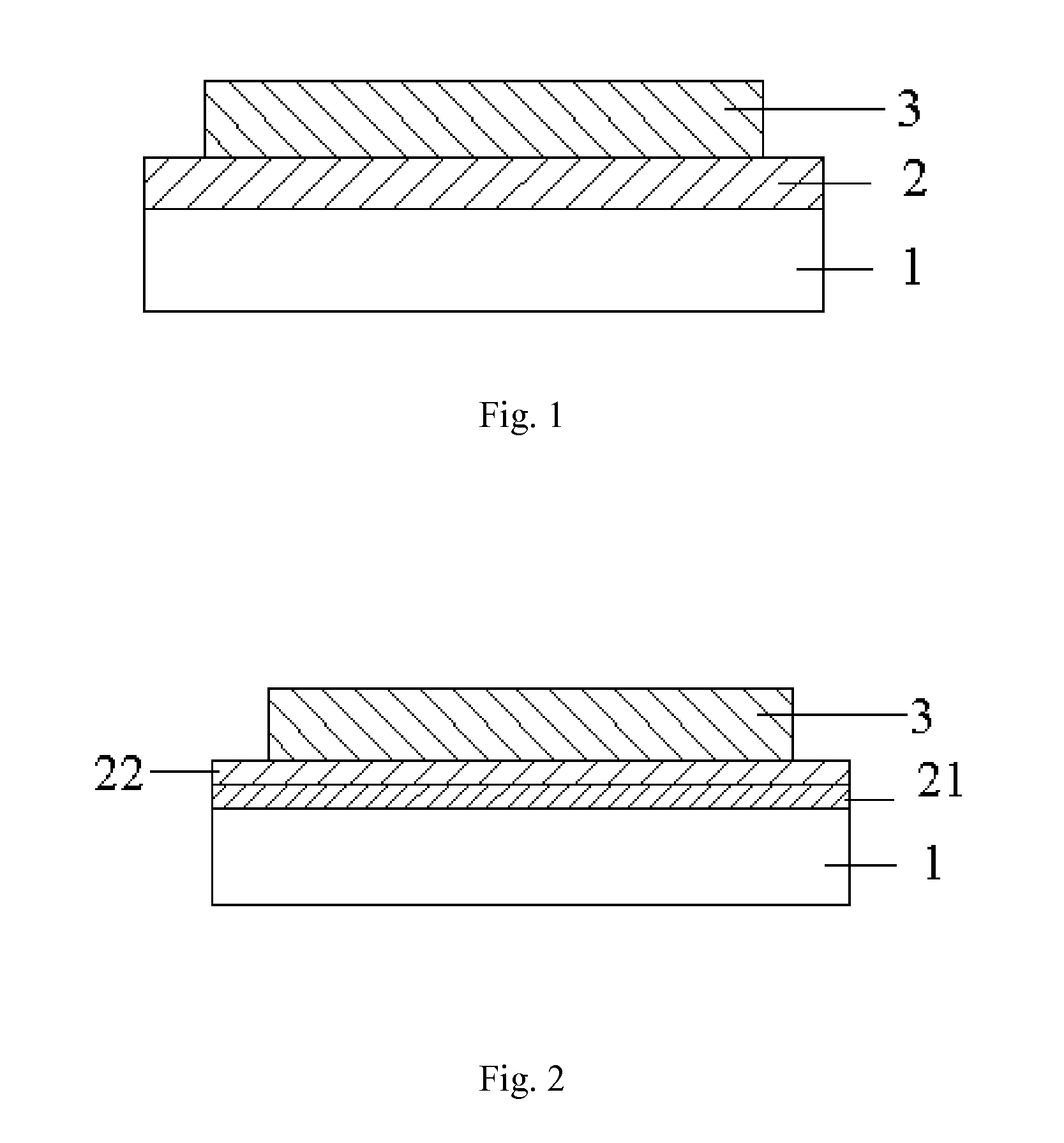
[0158]As shown in FIG. 1, the organic electroluminescent device 3 is embodied as a blue organic electroluminescence device. The spacer layer 2 adopts a single layer free radical ultraviolet curing agent-isocyanate thermal curing agent dual-curing system. The thin-film transistor 1 is an active driving circuit. A picture of the actual object is shown in FIG. 2.

[0159]The method of manufacture comprises the steps of:[0160]① ultrasonically cleaning the organic electroluminescent device by detergent, acetone solution, ethanol solution and deionized water, and drying the organic electroluminescence device by blowing dry nitrogen thereto;[0161]② preparing a thin-film transistor on a processed substrate;[0162]② stirring an adhesive material diluted by ethanol for 20 hours forming a mixture, wherein the adhesive material: ethanol is 1:10, applying the mixture onto a surface of the thin-film transistor in a spinning manner for a minute forming a spacer layer, wherein the spinning rate is 2000...

example 2

[0176]As shown in FIG. 1, the organic electroluminescent device 3 is embodied as a green organic electroluminescence device. The spacer layer 2 adopts a single layer free radical ultraviolet curing agent-epoxy resin thermal curing agent dual-curing system. The thin-film transistor 1 is an active driving circuit.

[0177]The method of manufacture comprises the steps of:[0178]① ultrasonically cleaning an organic electroluminescent device by detergent, acetone solution, ethanol solution and deionized water, and drying the organic electroluminescence device by blowing dry nitrogen thereto;[0179]② preparing a thin-film transistor on a processed substrate;[0180]③ stirring an adhesive material diluted by ethanol for 20 hours forming a mixture, wherein the adhesive material: ethanol is 1:10, applying the mixture onto a surface of the thin-film transistor in a spinning manner for a minute forming a spacer layer, wherein the spinning rate is 2000 rev / sec and the thickness of the spacer layer is ...

example 3

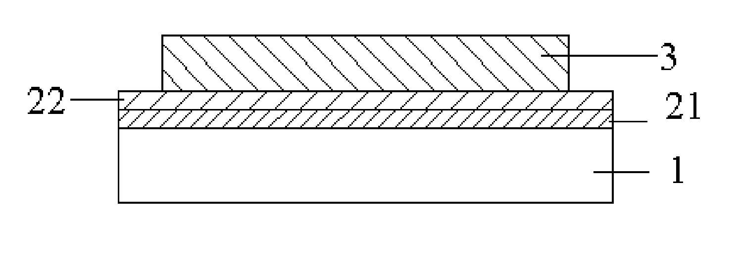
[0193]As shown in FIG. 1, the organic electroluminescent device 3 is embodied as a red organic electroluminescence device. The spacer layer 2 adopts a single layer cationic epoxy ultraviolet curing agent-amino resin thermal curing agent dual-curing system. The thin-film transistor 1 is an active driving circuit.

[0194]The method of manufacture comprises the steps of:[0195]① ultrasonically cleaning the organic electroluminescent device by detergent, acetone solution, ethanol solution and deionized water, and drying the organic electroluminescence device by blowing dry nitrogen thereto;[0196]② preparing a thin-film transistor on a processed substrate;[0197]③ stirring an adhesive material diluted by ethanol for 20 hours forming a mixture, wherein the adhesive material: ethanol is 1:10, applying the mixture onto a surface of the thin-film transistor in a spinning manner for a minute forming a spacer layer, wherein the spinning rate is 2000 rev / sec and the thickness of the spacer layer is...


PUM


Abstract

An active matrix organic electroluminescent device includes a thin-film transistor, an organic electroluminescent device, and a spacer layer deposited between the thin-film transistor and the organic electroluminescent device, wherein the spacer layer is made of adhesive for a dual curing system selected from the group consisting of ultraviolet curing-thermal curing, ultraviolet curing-microwave curing, ultraviolet curing-anaerobic curing, and ultraviolet curing-electron beam curing system. The present invention solves the poor adhesiveness between the thin-film transistor and the organic electroluminescent device, and improves the moisture and oxygen proof ability. The preparation method is simple, effective, and able to lower the cost and difficulty, and greatly improve the yield rate of the device.

Description

BACKGROUND OF THE PRESENT INVENTION[0001]1. Field of Invention[0002]The present invention relates to an organic optoelectronic device technology, and more particularly to an active matrix organic electroluminescent device and method of manufacture thereof.[0003]2. Description of Related Arts[0004]Optoelectronic technology is a rapid developing high-tech emerging industry after microelectronic technology. With the rapid development of optoelectronic technology, its related devices such as solar cells, optical imaging sensors, plasma display panels, electroluminescent displays, thin-film transistors, liquid crystal display panels and so on, have gradually developed, which greatly improve the people's living standard and quality of life. At the same time, the wide application of the optoelectronic information technology in various fields of social life also creates a growing market. Nowadays, the optoelectronic information industry has been regarded as one of the key development fields...

Claims


Application Information

Patent Timeline
IPC IPC(8): H01J1/62H01J9/22
CPCH01L27/3258H10K59/124
Inventor YU, JUNSHENGJIANG, YADONGZHONG, JIANLIN, HUI
Owner UNIV OF ELECTRONICS SCI & TECH OF CHINA
Why Eureka
Try Eureka