Electrode for electrochemical reaction and production process thereof
a technology of electrochemical reaction and electrode, which is applied in the direction of electrochemical machining apparatus, chemical/physical processes, metal/metal-oxide/metal-hydroxide catalyst, etc., can solve the problems of inability to find an industrial production process of porous and high-quality diamond electrode, inability to improve diamond quality, and extensive and intensive investigations. , to achieve the effect of increasing reaction efficiency, high quality and large surface area
- Summary
- Abstract
- Description
- Claims
- Application Information
AI Technical Summary
Benefits of technology
Problems solved by technology
Method used
Image
Examples
example 1
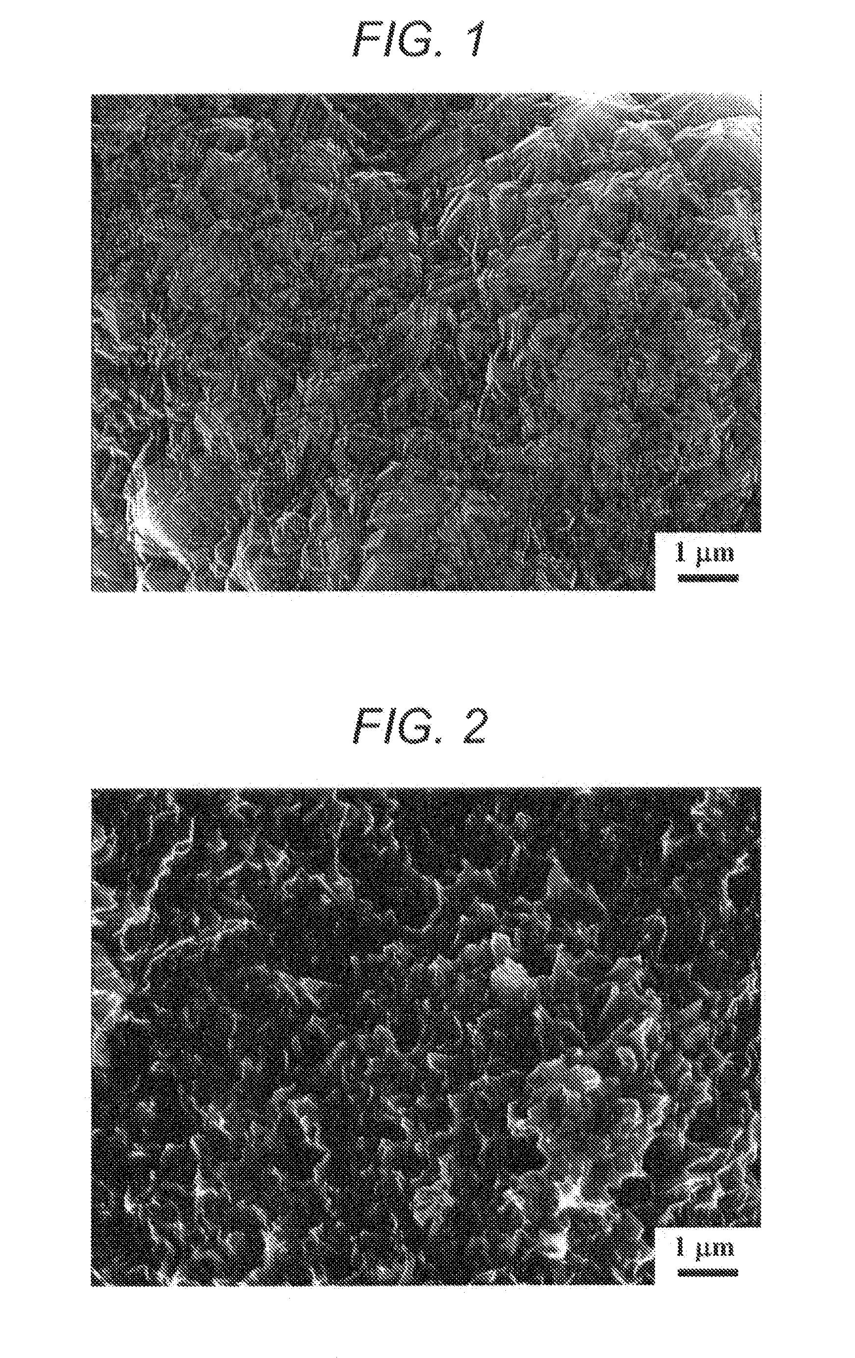
[0079]Diamond was deposited directly on a single-crystalline Si plate having a thickness of 1 mm as a substrate by using a hot filament CVD apparatus under the following conditions. The substrate surface was polished with a polishing agent composed of diamond fine particles (3 μm in diameter), thereby activating the surface and achieving nucleus formation, and the substrate was then installed in the hot filament CVD apparatus. Ethyl alcohol was used as a carbon source, and boron oxide wad dissolved therein in a concentration of 1,500 ppm. A hydrogen gas was allowed to flow at a rate of 0.01 L / min; a part thereof was by-passed into a carbon source container, thereby regulating the ethyl alcohol gas concentration to 0.5% by volume relative to hydrogen; a current was allowed to flow into the filaments while allowing these gases to flow into the apparatus; and the temperature was raised to 2,200 to 2,400° C. at which a carbon radical was formed. As a result of measuring the temperature ...
example 2
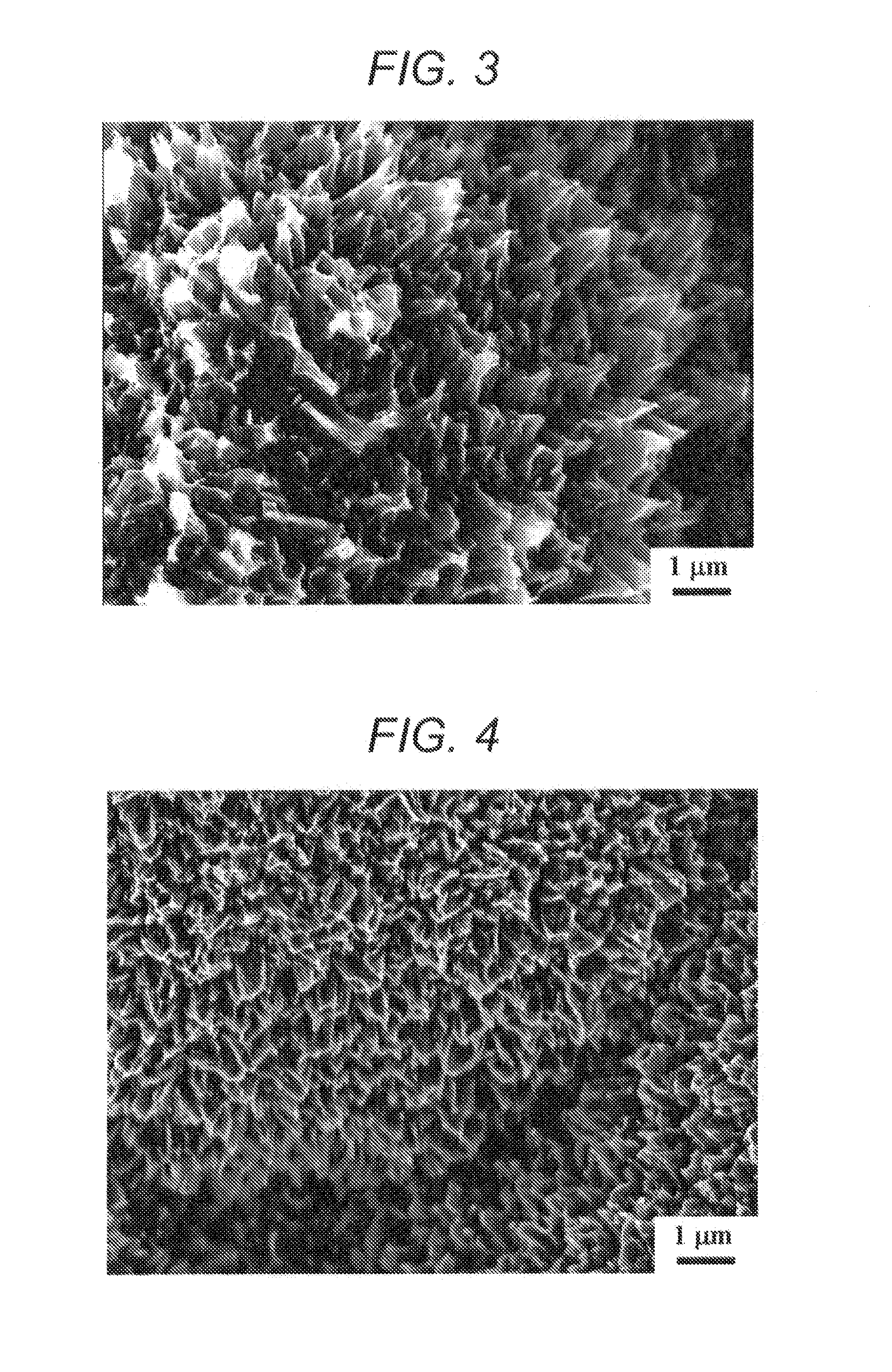
[0083]A 5 μm-thick diamond electrode fabricated in the same manner as in Example 1 was treated at 800° C. for 2 hours in a nitrogen flow containing 10% of a water vapor at 0.1 MPa. As a result, pores having a diameter of from 0.1 μm to 1 μm were formed on the electrode surface (see an electron microscopic photograph of FIG. 2). From the Raman spectrum of FIG. 7, it was found that a G band caused by sp2 carbon reduced, graphite-shaped carbon existing in boron-doped diamond (BDD) was selectively varnished, and a D / G ratio increased to 1.9.
[0084]Electrolysis was performed in the same manner as in Example 1. As shown by “800° C.” in the graph of FIG. 6, the results of the electrochemical measurement (cyclic voltammogram at 100 mV / s in 0.5 M sulfuric acid) reveal that an electrochemical double-layer capacity was 103 μF / cm2. This value increases to 10 times as compared with 11 μF / cm2 of the electrode which had not been subjected to a water vapor treatment.
example 3
[0085]A 5 μm-thick diamond electrode fabricated in the same manner as in Example 1 was treated at 900° C. for 1 hour in a nitrogen flow containing 10% of a water vapor at 0.1 MPa. As a result, irregularities of from 0.1 μm to 1 μm were formed on the electrode surface (see an electron microscopic photograph of FIG. 3). From the Raman spectrum of FIG. 7, it was found that a G band caused by sp2 carbon reduced, graphite-shaped carbon existing in BDD was selectively varnished, and a D / G ratio increased to 2.15.
[0086]Electrolysis was performed in the same manner as in Example 1. As shown by “900° C.” in the graph of FIG. 6, the results of the electrochemical measurement (cyclic voltammogram at 100 mV / s in 0.5 M sulfuric acid) reveal that an electrochemical double-layer capacity was 235 μF / cm2. This value increases to 20 times as compared with 11 μF / cm2 of the electrode which had not been subjected to a water vapor treatment.
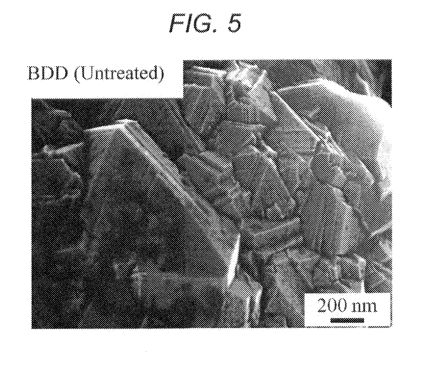
[0087]In this connection, an electron microscopic photograph of ...
PUM
| Property | Measurement | Unit |
|---|---|---|
| temperature | aaaaa | aaaaa |
| temperature | aaaaa | aaaaa |
| diameter | aaaaa | aaaaa |
Abstract
Description
Claims
Application Information


