Etch patterning of nanostructure transparent conductors

a transparent conductor and nano-structure technology, applied in the direction of insulated conductors, power cables, cables, etc., can solve the problems of difficult to adhere to metal oxide films, metal oxide films are fragile and prone to damage, and the application of metal oxide films on flexible substrates is severely limited

Active Publication Date: 2011-10-20
CHAMP GREAT INTL
View PDF4 Cites 102 Cited by
  • Summary
  • Abstract
  • Description
  • Claims
  • Application Information

AI Technical Summary

Benefits of technology

[0005]Accordingly, there remains a need in the art to provide transparent conductors having desirable electrical, optical and mechanical properties, in particular, transparent conductors that are adaptable to any substrates, and can be manufactured and patterned in a low-cost, high-throughput process.

Problems solved by technology

However, metal oxide films are fragile and prone to damage during bending or other physical stresses.
For certain substrates that are prone to adsorbing moisture such as plastic and organic substrates (e.g., polycarbonates), it may be problematic for a metal oxide film to adhere properly.
Applications of metal oxide films on flexible substrates are therefore severely limited.
In addition, vacuum deposition is a costly process and requires specialized equipment.
Moreover, the process of vacuum deposition is not conducive to forming patterns and circuits.
This typically results in the need for expensive patterning processes such as photolithography.
However, they generally have lower conductivity values and higher optical absorption (particularly at visible wavelengths) compared to the metal oxide films, and may lack chemical and long-term stability.

Method used


Image

  • Etch patterning of nanostructure transparent conductors
  • Etch patterning of nanostructure transparent conductors
  • Etch patterning of nanostructure transparent conductors

Examples


example 1

Synthesis of Silver Nanowires

[0116]Silver nanowires were synthesized by the reduction of silver nitrate dissolved in ethylene glycol in the presence of poly(vinyl pyrrolidone) (PVP) following the “polyol” method described in, e.g., Y. Sun, B. Gates, B. Mayers, & Y. Xia, “Crystalline silver nanowires by soft solution processing”, Nanoletters, (2002), 2(2) 165-168. A modified polyol method, described in U.S. application Ser. No. 11 / 766,552, in the name of Cambrios Technologies Corporation, produces more uniform silver nanowires at higher yields than does the conventional “polyol” method. This application is incorporated by reference herein in its entirety.

example 2

Preparation of a Transparent Conductor

[0117]An Autoflex EBG5 polyethylene terephthalate (PET) film 5 μm thick was used as a substrate. The PET substrate is an optically clear insulator. The light transmission and haze of the PET substrate are shown in Table 2. Unless specified otherwise, the light transmission was measured using the methodology in ASTM D1003.

[0118]An aqueous dispersion of silver nanowires was first prepared. The silver nanowires were about 70 nm to 80 nm in width and around 8 μm in length. The concentration of the silver nanowires (AgNW) was about 0.5% w / v of the dispersion, resulting in an optical density of about 0.5 (measured on a Molecular Devices Spectra Max M2 plate reader). The dispersion was then coated on the PET substrate by allowing the nanowires to sediment onto the substrate. As understood by one skilled in the art, other coating techniques can be employed, e.g., flow metered by a narrow channel, die flow, flow on an incline and the like. It is further...

example 3

Acid-Etching (1)

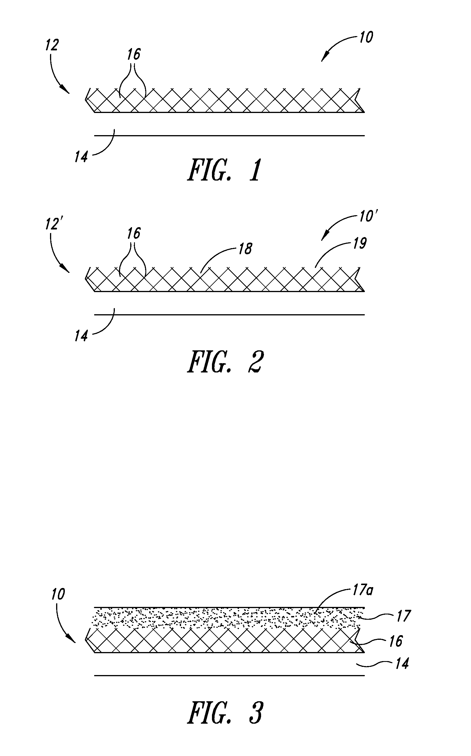
[0127]A conductive silver nanowires layer was first formed on a PET substrate. A UV-curable acrylate was deposited on the nanowire layer according to a pattern. The matrix was allowed to dry and partially cured. The matrix was typically about 50 nm-300 nm thick. Surface conductivity was detected in the areas protected by the matrix as well as in the areas unprotected by the matrix.

[0128]The transparent conductor sheet was then exposed to an acid-etching solution, which included 1% HNO3, 1% NaNO3 and 5 ppm of KMnO4.

[0129]Within one minute, the etching of the silver nanowires had begun from a region adjacent to an area protected by the matrix. The dissolution and disruption of the nanowire layer was evident in the area unprotected by the matrix.

[0130]Two minutes into the etching, more unprotected silver nanowires were dissolved and a well-defined pattern emerged. At the end of four minutes, all the unprotected silver nanowires had been etched and removed by rinsing the...


PUM

PropertyMeasurementUnit
hazeaaaaaaaaaa
viscosityaaaaaaaaaa
diameteraaaaaaaaaa

Abstract

A patterned transparent conductor including a conductive layer coated on a substrate is described. More specifically, the transparent conductor can be patterned by screen-printing an acidic etchant formulation on the conductive layer. A screen-printable etchant formulation is also disclosed.

Description

CROSS-REFERENCES TO RELATED APPLICATIONS[0001]This application claims the benefit under 35 U.S.C. §119(e) of U.S. Provisional Patent Application No. 61 / 316,770 filed Mar. 23, 2010, and U.S. Provisional Patent Application No. 61 / 391,564 filed Oct. 8, 2010; these provisional applications are incorporated herein by reference in their entireties.BACKGROUNDDescription of the Related Art[0002]Transparent conductors refer to thin conductive films coated on high-transmittance surfaces or substrates. Transparent conductors may be manufactured to have surface conductivity while maintaining reasonable optical transparency. Such surface conducting transparent conductors are widely used as transparent electrodes in flat liquid crystal displays, touch panels, electroluminescent devices, and thin film photovoltaic cells, as anti-static layers and as electromagnetic wave shielding layers.[0003]Currently, vacuum deposited metal oxides, such as indium tin oxide (ITO), are the industry standard materi...

Claims


Application Information

Patent Timeline
Patent Type & Authority Applications(United States)
IPC IPC(8): H01B13/00C09K13/06C09K13/00B82Y99/00
CPCB82Y10/00H01B1/22H01L31/022466H05K1/097C23F1/30H05K2201/026C23F1/00C23F1/02H05K3/06H01B5/00H01B7/00H01B9/00H01B11/00H01B12/00H01B17/02H01B19/00
Inventor WINOTO, ADRIANWOLK, JEFFREY
Owner CHAMP GREAT INTL
Why Eureka
Try Eureka