Semiconductor display device and driving method the same

a semiconductor display and semiconductor technology, applied in static indicating devices, instruments, sustainable buildings, etc., can solve the problems of short continuous operation time, low versatility, and low power consumption, so as to reduce power consumption, and prevent quality loss of images

Active Publication Date: 2011-11-03
SEMICON ENERGY LAB CO LTD
View PDF6 Cites 58 Cited by
  • Summary
  • Abstract
  • Description
  • Claims
  • Application Information

AI Technical Summary

Benefits of technology

[0021]In one embodiment of the present invention, driving frequency when a still image is display can be lower than driving frequency when a moving image is displayed at the time of an input of the positional information to a semiconductor display device. Therefore, a semiconductor display device having a touch panel, which can prevent quality loss of an image and can reduce power consumption, can be achieved. Further, a driving method of a semiconductor display device which can prevent quality loss of an image and can reduce power consumption can be achieved.

Problems solved by technology

In particular, when a portable electronic device such as a cellular phone is used, large power consumption of a semiconductor display device having a touch panel or a photosensor leads to a disadvantage of short continuous operation time; therefore, low power consumption is required.
However, it is necessary to limit the kinds of liquid crystal materials in order to achieve the above-mentioned structure in Patent Document 1; therefore, versatility is low.
In addition, display layers corresponding to their respective colors are stacked in the above-described liquid crystal display panel in order to display a full color image; therefore, loss of light inside the panel is large, and display is dark.

Method used


Image

  • Semiconductor display device and driving method the same
  • Semiconductor display device and driving method the same
  • Semiconductor display device and driving method the same

Examples


embodiment 1

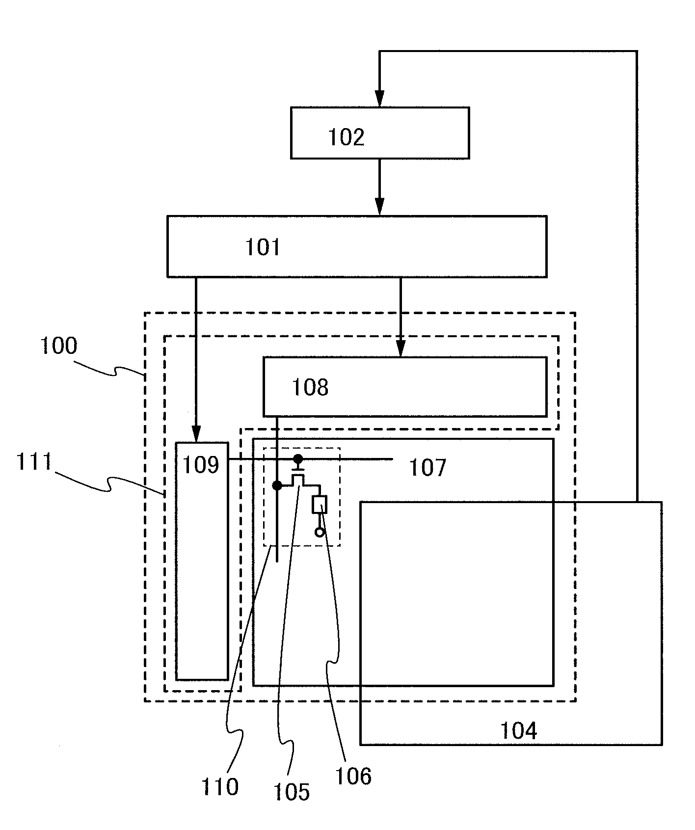
[0041]FIG. 1 is a block diagram illustrating a structure of a semiconductor display device according to one embodiment of the present invention. Note that in the block diagram in this specification, circuits are classified in accordance with their functions and separated blocks are illustrated. However, it is difficult to classify actual circuits according to their functions completely and it is possible for one circuit to have a plurality of functions.

[0042]A semiconductor display device illustrated in FIG. 1 includes a panel 100, a display control circuit 101, a CPU 102, and a touch panel 104. Further, the semiconductor display device according to one embodiment of the present invention may include a touch panel control circuit.

[0043]The panel 100 includes a pixel portion 107 provided with pixels 110 each including a transistor 105 and a display element 106, and a driver circuit 111 which controls operation of the pixel portion 107, such as a signal line driver circuit 108, a scan...

embodiment 2

[0074]In this embodiment, in the semiconductor display device illustrated in FIG. 1, a driving signal and a power supply potential which are transmitted from the display control circuit 101 to the driver circuit 111 in a period in which a still image is displayed will be described with reference to FIG. 4.

[0075]A start signal SP, a clock signal CK, and a power supply potential Vp are input to the display control circuit 101. In addition, a control signal GDCTL and a control signal SDCTL are input from the CPU 102 to the display control circuit 101. The control signal GDCTL is a signal for controlling drive of the scan line driver circuit 109 and the control signal SDCTL is a signal for controlling drive of the signal line driver circuit 108. The display control circuit 101 supplies a signal or potential which is input such as the start signal SP, the clock signal CK, or the power supply potential Vp to the scan line driver circuit 109 or the signal line driver circuit 108 in accorda...

embodiment 3

[0093]In this embodiment, an example of a shift register which can be used in a scan line driver circuit and a signal line driver circuit of the semiconductor display device described in the above embodiment will be described.

[0094]FIGS. 5A and 5B each illustrate an example of the structure of the shift register in this embodiment.

[0095]The shift register illustrated in FIG. 5A is formed using P unit sequential circuits 10 (P is a natural number of 3 or more). In FIG. 5A, the P unit sequential circuits 10 are illustrated as unit sequential circuits FF_1 to FF_P.

[0096]A start signal ST and a reset signal Res are input to each of the unit sequential circuits FF_1 to FF_P.

[0097]Further, a clock signal CK1, a clock signal CK2, and a clock signal CK3 are input to each of the unit sequential circuits FF_1 to FF_P. As the clock signal CK1, the clock signal CK2, and the clock signal CK3, for example, any three of a first clock signal (also referred to as CLK1), a second clock signal (also r...


PUM


Abstract

It is an object to provide a semiconductor display device having a touch panel, which can reduce power consumption. The semiconductor display device includes a panel which is provided with a pixel portion and a driver circuit which controls an input of the image signal to the pixel portion, and a touch panel provided in a position overlapping with the panel in the pixel portion. The pixel portion includes a display element configured to perform display in accordance with voltage of the image signal to be input, and a transistor configured to control retention of the voltage. The transistor includes an oxide semiconductor in a channel formation region. The driving frequency of the driver circuit, that is, the number of writing operations of the image signal for a certain period is changed in accordance with an operation signal from a touch panel.

Description

TECHNICAL FIELD[0001]The present invention relates to an active-matrix semiconductor display device using a transistor and a driving method thereof.BACKGROUND ART[0002]A touch panel is a position input device which can detect a position indicated with a finger, a stylus, or the like and can generate a signal including the positional information. A display device which is obtained in such a manner that a touch panel overlaps with an image display area is referred to as a touch screen, and the display device can display an image in an image display region and can obtain as information which position in the image display region a user indicates. In addition, an example of a touch screen includes a touch screen in which a photoelectric conversion element called a photosensor is provided in an image display region and a position indicated by a user is detected by intensity of light. The touch screen has both functions as a position input device and as a display device; therefore, the tou...

Claims


Application Information

Patent Timeline
Patent Type & Authority Applications(United States)
IPC IPC(8): G09G3/32G06F3/038G06F3/041
CPCG06F1/3265G06F3/0412G06F3/044G02F1/13338G09G3/3688Y02B60/1242G06F3/045G06F3/0446G09G3/3677G09G2300/0426G09G2330/021G09G2310/0286G09G2310/08G09G3/3648G09G2360/14Y02D10/00
Inventor YAMAZAKI, SHUNPEIKOYAMA, JUN
Owner SEMICON ENERGY LAB CO LTD
Why Eureka
Try Eureka