
Directional solid phase crystallization of thin amorphous silicon for solar cell applications

a technology of solar cells and solid phase crystallization, which is applied in the direction of crystal growth process, sustainable manufacturing/processing, final product manufacturing, etc., can solve the problems of high surface recombination velocity of minority charge carriers, and process complexity. complex gaseous diffusion process

Inactive Publication Date: 2011-11-17
APPLIED MATERIALS INC
View PDF0 Cites 4 Cited by
  • Summary
  • Abstract
  • Description
  • Claims
  • Application Information

AI Technical Summary

Benefits of technology

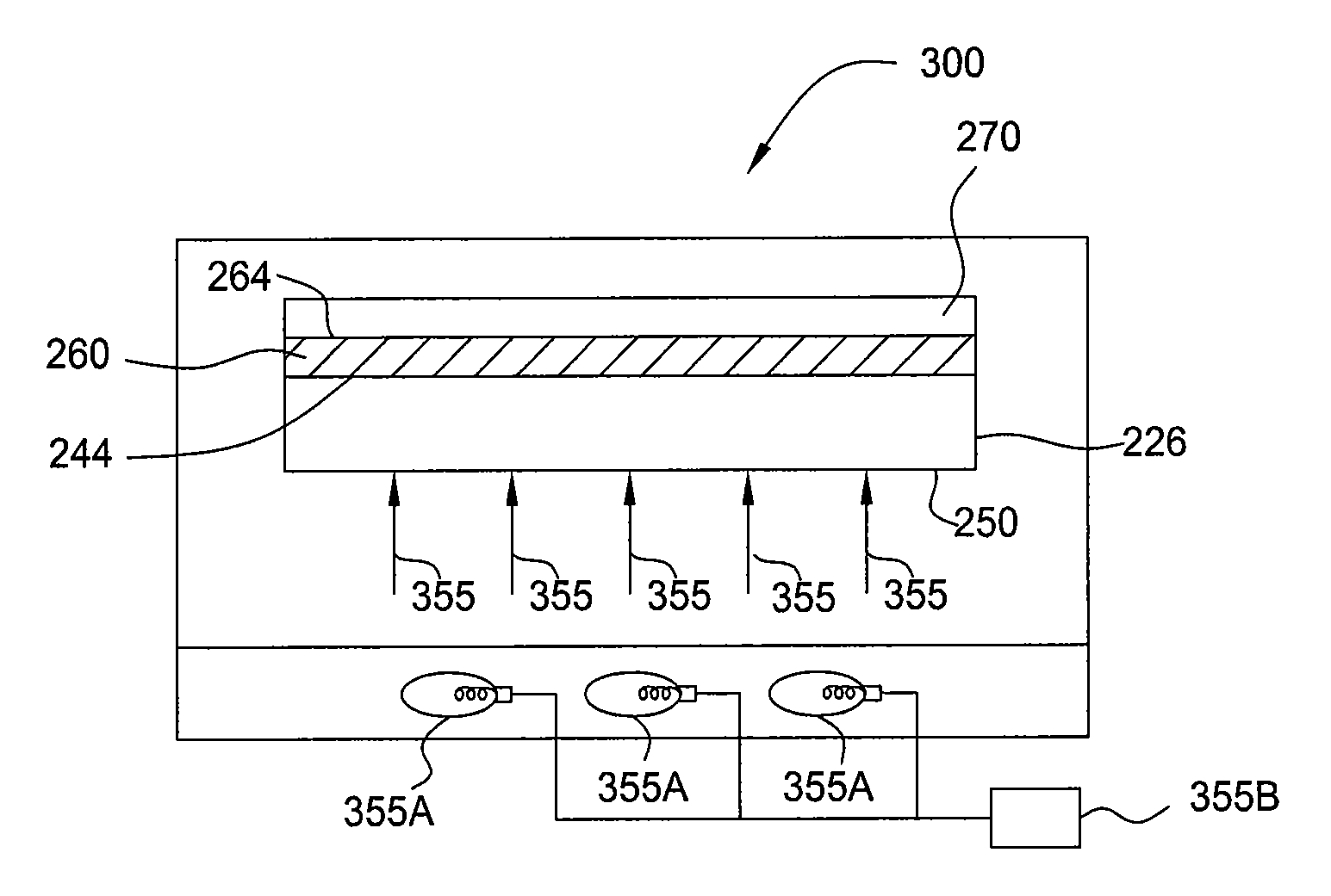
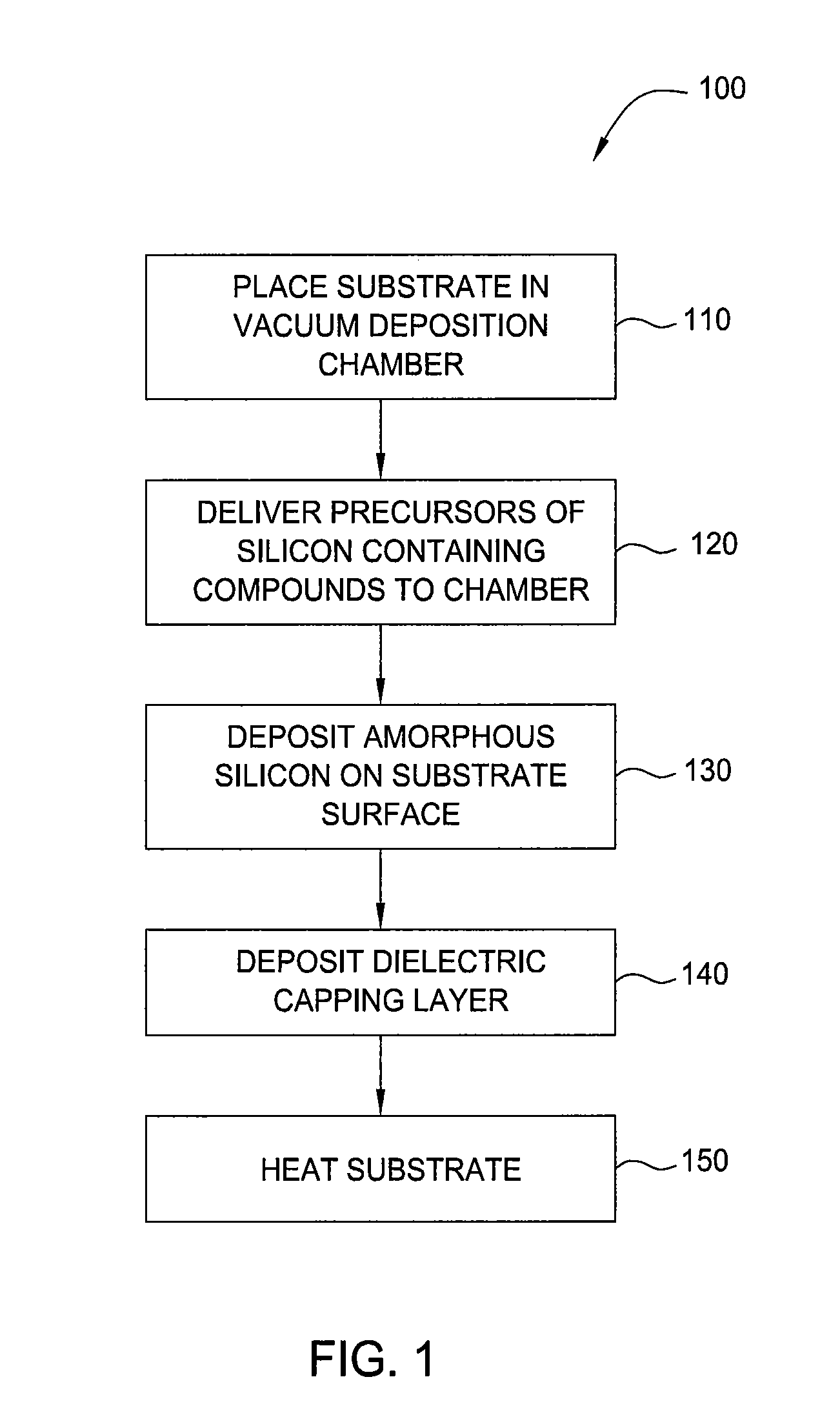
[0013]Embodiments of the invention may further provide a method of heat treating a crystalline silicon substrate to form a p-n junction, comprising depositing an amorphous silicon film on a first surface of the crystalline silicon substrate, wherein the first surface of the crystalline silicon substrate is generally opposite to second surface, depositing a dielectric layer over the amorphous silicon film, and heating the crystalline silicon substrate and the amorphous silicon film to a temperature that is sufficient to crystallize the amorphous silicon film, wherein the heating creates a temperature gradient between the second surface and the first surface so that a temperature of the first surface is higher than a temperature of a point within the amorphous silicon film that is a distance from the first surface.

Problems solved by technology

Such handling of the substrates inevitably results in breakage of some of the silicon substrates because the substrates are relatively thin, such as 0.3 mm thick or less.
Although phosphorous diffusion of the phosphorous-doped, n-type silicon material for solar junction formation may be created by the furnace type diffusion / annealing processes discussed above, these processes require performing complex gaseous diffusion processes that require many additional pre-cleaning, post-cleaning, etching, and stripping steps.
The use of such prior art p-n junction formation and surface passivation techniques for solar cell fabrication is expensive and can result in a defective interface between the dielectric passivation layer and the doped substrate, leading to a high surface recombination velocity for the minority charge carriers.
Moreover, using gaseous diffusion / annealing processes in a furnace, as previously described, typically results in the doping of both sides of the silicon substrate.

Method used


Image

  • Directional solid phase crystallization of thin amorphous silicon for solar cell applications
  • Directional solid phase crystallization of thin amorphous silicon for solar cell applications
  • Directional solid phase crystallization of thin amorphous silicon for solar cell applications

Examples


example 1

[0048]In one example, a 100 Å thick amorphous silicon film was deposited via plasma enhanced chemical vapor deposition onto a crystalline silicon substrate with a phosphorous doping concentration of 1.5×10²¹ atoms / cm3. A 900 Å thick silicon nitride film was then deposited over the phosphorous doped amorphous silicon film in the same chamber. The resulting structure was annealed via RTP at 950° C. for 120 seconds in a nitrogen environment. The phosphorous concentration in contact with the silicon nitride layer remained heavily doped. The phosphorous in contact with the crystalline substrate diffused into the substrate resulting in a p-n junction depth of 900 Å. The resulting structure had a dopant profile with a high concentration of dopant collected at the interface between the silicon, nitride layer and the silicon layer decreasing to a lower concentration of dopant at the p-n junction.

example 2

[0049]In another example, a 100 Å thick amorphous silicon film was deposited via plasma enhanced chemical vapor deposition onto a crystalline silicon substrate with a phosphorous doping concentration of 1.5×10²¹ atoms / cm3. A 900 Å thick silicon nitride film was then deposited over the phosphorous doped amorphous silicon film in the same chamber. The resulting structure was annealed via RTP at 1,000° C. for 120 seconds in a nitrogen environment. The phosphorous concentration in contact with the silicon nitride layer remained heavily doped. The phosphorous in contact with the crystalline substrate diffused into the substrate resulting in a p-n junction depth of 1,350 Å. The resulting structure had a dopant profile with a high concentration of dopant collected at the interface between the silicon nitride layer and the silicon layer decreasing to a lower concentration of dopant at the p-n junction.

[0050]Although the invention has been described in accordance with certain embodiments and...


PUM

PropertyMeasurementUnit
concentrationaaaaaaaaaa
temperatureaaaaaaaaaa

Abstract

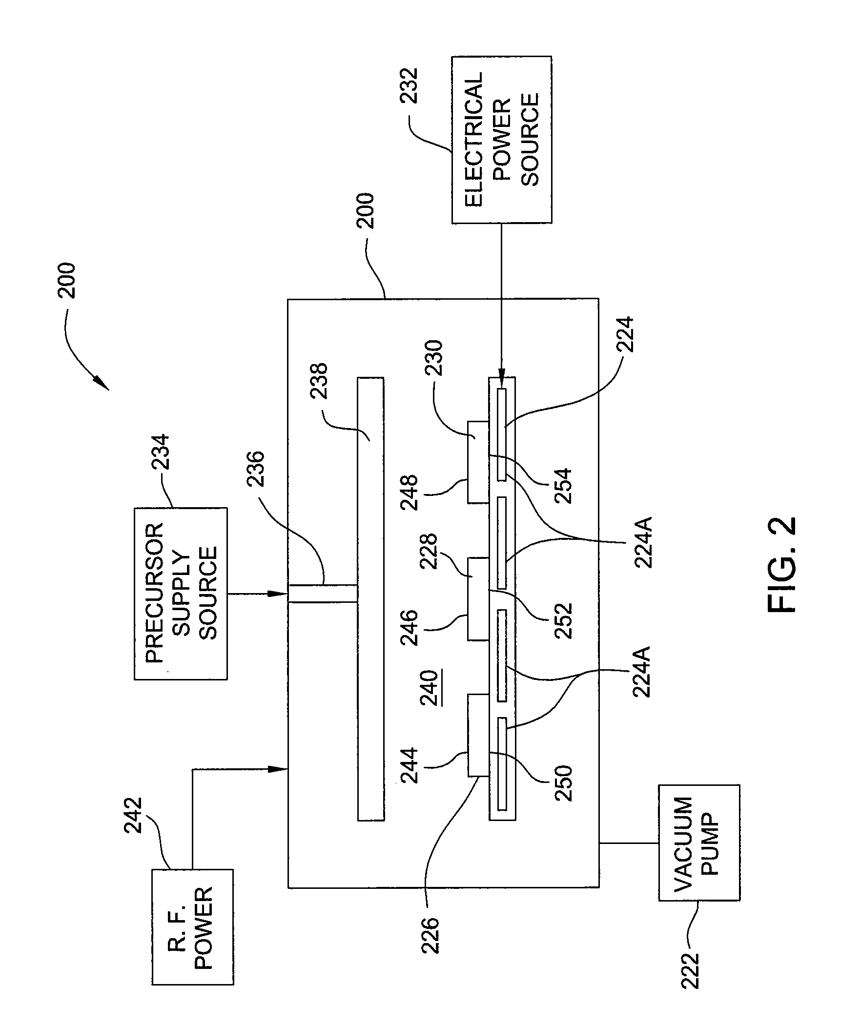
Embodiments of the invention provide a system for heat treating a substrate which includes a first processing chamber having a first processing region coupled with a precursor source assembly configured to deliver a silicon containing gas to an upper surface of a substrate disposed within the first processing region in order to form an amorphous silicon film on the upper surface. The system further includes a substrate support having a heating element configured to heat the substrate to a temperature sufficient to crystallize the amorphous silicon film by solid phase crystallization and to create a temperature gradient in which a temperature at the lower surface of the substrate is greater than a temperature at the upper surface of the amorphous silicon film and the temperature gradient is within a range from about 2° C. to about 10° C.

Description

CROSS-REFERENCE TO RELATED APPLICATIONS[0001]This application is a divisional application of U.S. Ser. No. 12 / 507,761 (APPM / 012161), filed Jul. 22, 2009, and issued as U.S. Pat. No. 7,981,778, which claims benefit of U.S. Ser. No. 61 / 082,812 (APPM / 012161L), filed Jul. 22, 2008, and U.S. Ser. No. 61 / 097,793 (APPM / 012161L02), filed Sep. 17, 2008, which are all herein incorporated by reference in their entirety.BACKGROUND OF THE INVENTION[0002]1. Field of the Invention[0003]Embodiments of the invention generally relate to the fabrication of silicon solar cells and, more particularly, to a method of converting a layer of amorphous silicon deposited on a sheet of crystalline silicon to crystalline silicon by solid phase epitaxy.[0004]2. Description of the Related Art[0005]Solar cells are photovoltaic (PV) devices that convert sunlight directly into electrical power. Solar cells typically have one or more p-n junctions. Each junction comprises two different regions within a semiconductor ...

Claims


Application Information

Patent Timeline
Patent Type & Authority Applications(United States)
IPC IPC(8): C30B1/06
CPCH01L21/02381H01L21/02433H01L21/02532H01L21/02573H01L21/02609Y10T117/10H01L31/068H01L31/1804H01L31/1872Y02E10/547H01L21/0262Y02P70/50
Inventor RANA, VIRNEDRA V.BACHRACH, ROBERT Z.
Owner APPLIED MATERIALS INC
Learn More