Transparent Photonic Integrated Circuit

a photonic integrated circuit and transparent technology, applied in the field of photonic integrated circuits, can solve the problems of limited wavelength range, limited 1 db optical bandwidth to 50 nm, and considerable challenges, and achieve the effects of efficient multiplexing, efficient emission or detection of optical signals, and efficient coupling of optical signals received

Active Publication Date: 2011-11-17
INTERUNIVERSITAIR MICRO ELECTRONICS CENT (IMEC VZW) +1
View PDF4 Cites 31 Cited by
  • Summary
  • Abstract
  • Description
  • Claims
  • Application Information

AI Technical Summary

Benefits of technology

[0010]It is an object of embodiments of the present invention to provide good transceivers, that allow efficient emission or detection of optical signals, while at the same time having efficient coupling of optical signals received in or emitted from the transceiver respectively. It is an advantage of embodiments according to the present invention that efficient multiplexing between radiation to and from the transceiver can be obtained. It is an advantage of embodiments according to the present invention that multiplexing between radiation to and from the transceiver can be obtained without the need for a grating, e.g. by using a transparent component for emitting or detecting radiation in a particular wavelength range while allowing transmission of the radiation through the transparent component for radiation to be processed in the system in another wavelength range.

Problems solved by technology

Using high index contrast photonic integrated circuits for communication applications however also bring along considerable challenges, especially regarding the efficient fiber-to-chip coupling and polarization independent operation of the photonic integrated circuit, and the need for handling widely spaced wavelength bands.
However, the 1 dB optical bandwidth is limited to 50 nm.
While this allows reducing the polarization dependent loss, it also only works over a limited wavelength range, which is insufficient for Fiber-to-the-Home (FTTH) transceiver applications.
Moreover, the two-dimensional grating approach introduces a decrease in fiber-to-chip coupling efficiency.

Method used


Image

  • Transparent Photonic Integrated Circuit
  • Transparent Photonic Integrated Circuit
  • Transparent Photonic Integrated Circuit

Examples


Embodiment Construction

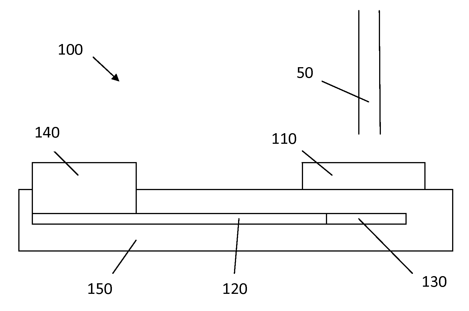
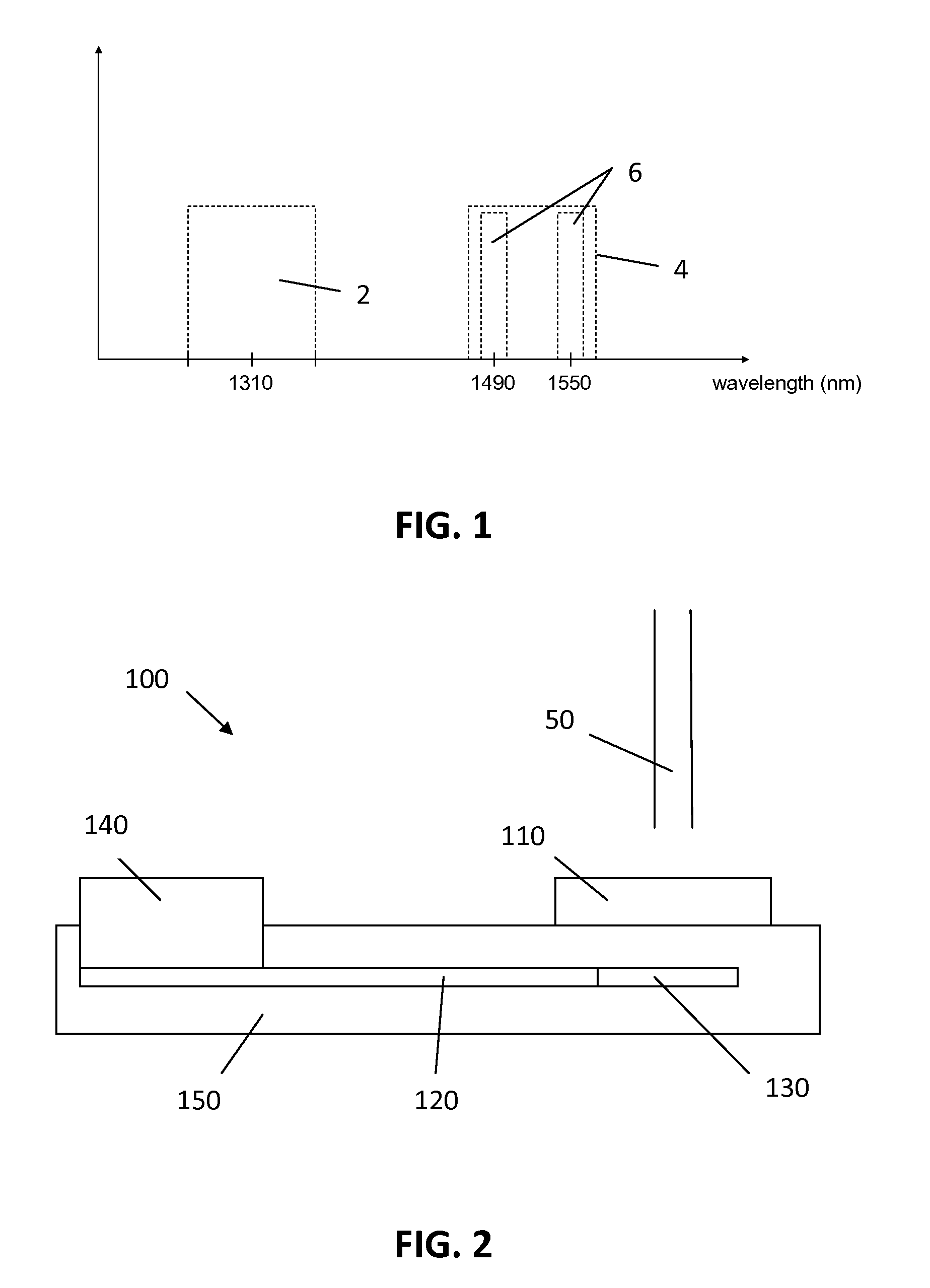
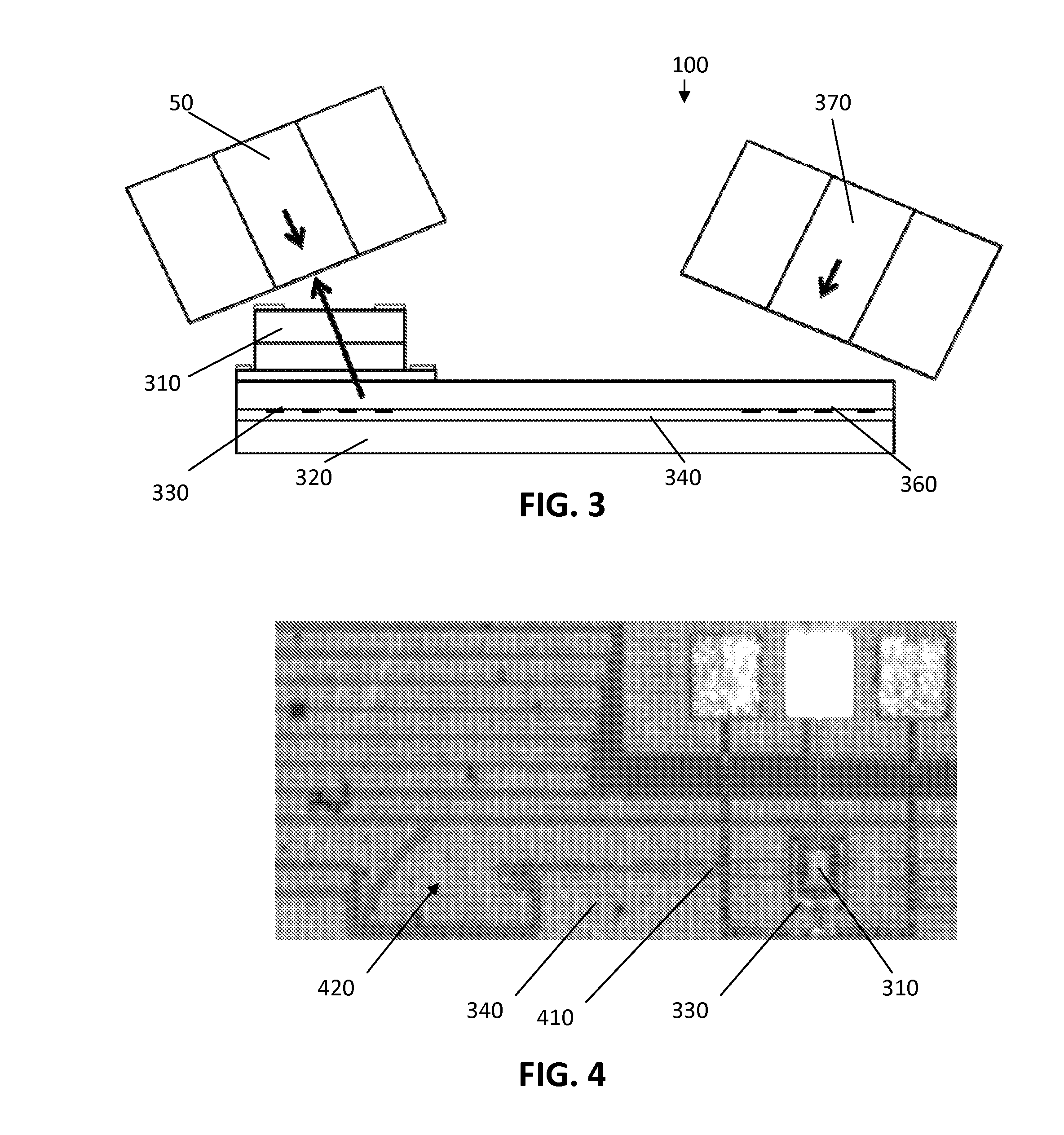
a transparent vertically emitting laser, in accordance with an embodiment.

[0038]FIG. 10 illustrates the reflectivity of a mirror of a vertically emitting laser, in accordance with an embodiment.

[0039]FIG. 11 shows an example of an optical system using a vertically emitting laser and integrated Ge detector, in accordance with an embodiment.

[0040]FIG. 12 shows an example of an optical system using an edge emitting laser and integrated Ge detector, in accordance with an embodiment.

[0041]FIGS. 13a-b show cross-sections of a distributed feedback laser (FIG. 13a) and a Fabry-Pérot laser (FIG. 13b), in accordance with an embodiment.

[0042]FIG. 14 shows an optical system using an edge emitting laser and a III-V detector, in accordance with an embodiment.

[0043]FIG. 15 shows a photonics device, in accordance with an embodiment.

[0044]The drawings are merely schematic and are not meant to be limiting. In the drawings, the size of some of the elements may be exaggerated and not drawn on scale for...


PUM

PropertyMeasurementUnit
transparentaaaaaaaaaa
wavelength bandaaaaaaaaaa

Abstract

Photonic structures and methods of operating the photonic structures are disclosed. In one embodiment, the photonic structure includes a detector configured to detect radiation of a first wavelength range. The radiation of the first wavelength range is received from an external radiation guide, and the detector is substantially transparent to radiation of a second wavelength range that differs from the first wavelength range. The photonic structure further includes a coupling structure configured to free space couple out of the photonic structure radiation of the second wavelength range. The photonic structure further includes a guiding structure configured to optically guide the radiation of the second wavelength range through the detector.

Description

CROSS-REFERENCE TO RELATED APPLICATIONS[0001]This application claims priority to U.S. Provisional Application Ser. No. 61 / 334,057 filed May 12, 2010 and European Patent Application Serial No. EP 10177399.2 filed Sep. 17, 2010. The contents of each are hereby incorporated by reference.FIELD OF THE INVENTION[0002]The invention relates to the field of photonic integrated circuits and methods of manufacturing and using them. More particularly, the present invention relates to a system comprising a photonic integrated circuit comprising a photodetector, such as a III-V semiconductor photodetector, a radiation source, such as a III-V semiconductor laser, and to optical emitters, receivers or transceivers wherein such optical elements are integrated on a photonic integrated circuit, such as a silicon based photonic integrated circuit.BACKGROUND[0003]In the Fiber-to-the-Home (FTTH) market, two technologies are competing: passive optical networks (PON) and Ethernet-based point-to-point netwo...

Claims


Application Information

Patent Timeline
Patent Type & Authority Applications(United States)
IPC IPC(8): G01N21/25G01J1/04
CPCG02B6/12004G02B6/124G02B6/34H01S5/18361G02B6/4246H01S5/02248G02B6/4214H01S5/02325
Inventor VERMEULEN, DIEDRIKROELKENS, GUNTHER
Owner INTERUNIVERSITAIR MICRO ELECTRONICS CENT (IMEC VZW)
Why Eureka
Try Eureka