Semiconductor device

a technology of semiconductors and devices, applied in the direction of semiconductor devices, electrical equipment, transistors, etc., can solve the problems of increasing power consumption increasing heat generation due to through current, etc., and achieves the effect of suppressing power consumption, low off-state current, and reducing through curren

Active Publication Date: 2011-11-17
SEMICON ENERGY LAB CO LTD
View PDF5 Cites 55 Cited by
  • Summary
  • Abstract
  • Description
  • Claims
  • Application Information

AI Technical Summary

Benefits of technology

[0020]In the semiconductor device according to one embodiment of the present invention, the threshold voltage of the p-channel transistor or the n-channel transistor which forms the complementary logic circuit is controlled by the potential supplied to the second gate electrode or the substrate potential. Therefore, when the potential of the gate electrode of the p-channel transistor or the n-channel transistor is switched from a high level to a low level or from a low level to a high level, one of the transistors can be made to turn off or a period where both of the transistors are turned on can be shortened. Thus, the through current which flows through channel formation regions of the p-channel transistor and the n-channel transistor can be reduced. Further, in the semiconductor device according to one embodiment of the present invention, the potential of the second gate electrode or the substrate potential can be held by the transistor with an extremely low off-state current; therefore, the threshold voltage which is set in accordance with the potential can be maintained even when a potential is not always supplied to the second gate electrode or a potential is not always supplied to a substrate.
[0021]Therefore, in the semiconductor device according to one embodiment of the present invention, a through current can be reduced; thus, power consumption can be suppressed. Alternatively, in the semiconductor device according to one embodiment of the present invention, a through current can be reduced; thus, heat generation can be suppressed.

Problems solved by technology

The power consumption due to the through current increases as the integration degree of an integrated circuit including a logic circuit is increased.
Further, when the driving frequency of the integrated circuit is increased up to the unit of gigahertz (GHz), the amount of heat generation due to a through current becomes large.

Method used


Image

  • Semiconductor device
  • Semiconductor device
  • Semiconductor device

Examples


embodiment 1

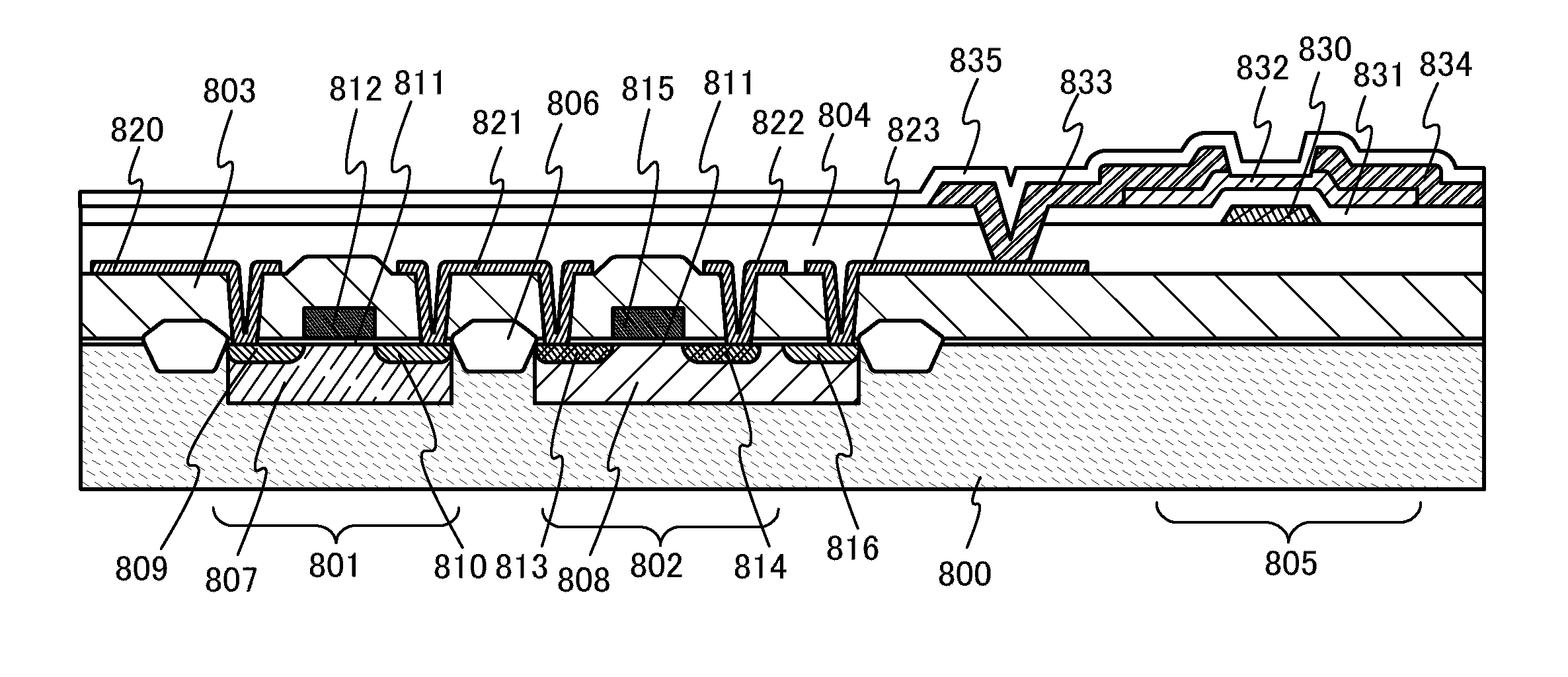
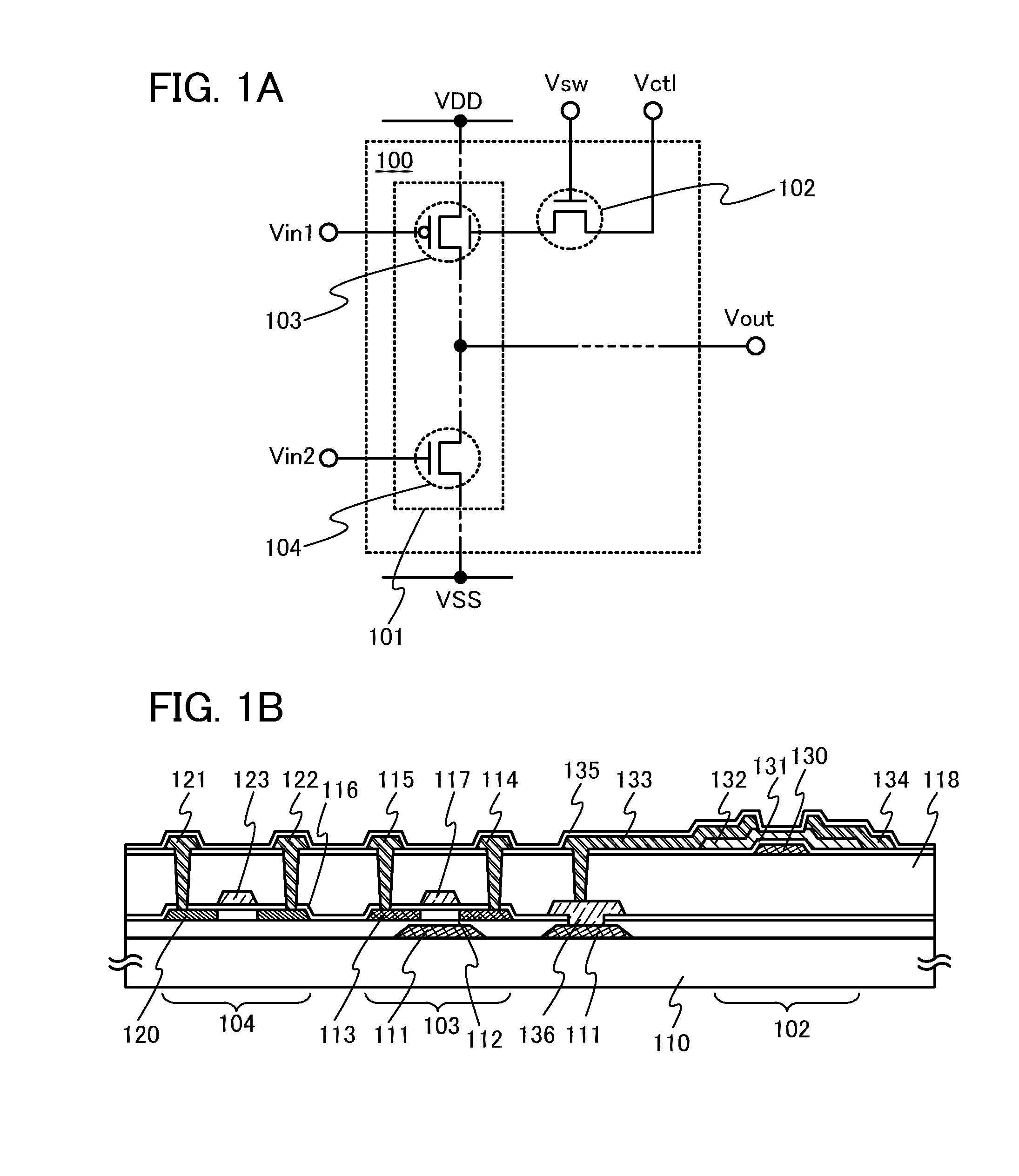
[0041]FIG. 1A shows an example of the structure of a logic circuit which is used in a semiconductor device according to one embodiment of the present invention.

[0042]A logic circuit 100 in FIG. 1A includes a logic portion 101 for performing logical operation and a transistor 102 which functions as a switching element. The logic portion 101 includes at least a p-channel transistor 103 and an n-channel transistor 104. In the logic portion101, logical operation to be performed is uniquely determined in accordance with the number and connection structure of the p-channel transistor 103 and the n-channel transistor 104. Then, one output value can be obtained from a plurality of input values by the logical operation which is performed in the logic portion 101.

[0043]Note that the input value means a logical value represented by a potential Vin of an input signal inputted into the logic circuit 100. Further, the output value means a logical value represented by a potential Vout of an output...

embodiment 2

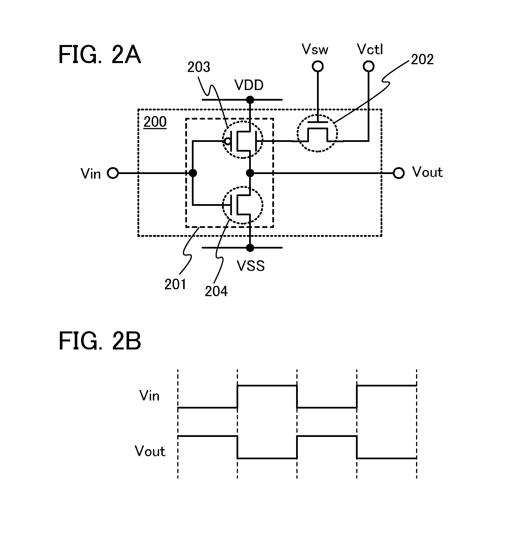
[0092]In this embodiment, another example of the structure of a logic circuit which is used in a semiconductor device according to one embodiment of the present invention will be shown.

[0093]A logic circuit 200 in FIG. 2A includes a logic portion 201 for performing logical operation and a transistor 202 with a low off-state current, which functions as a switching element. The logic portion 201 includes a p-channel transistor 203 and an n-channel transistor 204. FIG. 2A shows, as an example, the case where the logic portion 201 is an inverter including the p-channel transistor 203 and the n-channel transistor 204.

[0094]Specifically, in the logic portion 201, a gate electrode of the p-channel transistor 203 and a gate electrode of the n-channel transistor 204 are connected to each other. A potential Vin of an input signal inputted into the logic circuit 200 is supplied to the gate electrode of the p-channel transistor 203 and the gate electrode of the n-channel transistor 204. Further...

embodiment 3

[0111]In this embodiment, another example of the structure of a logic circuit which is used in a semiconductor device according to one embodiment of the present invention will be shown.

[0112]A logic circuit 300 in FIG. 6A includes a logic portion 301 for performing logical operation and a transistor 302 and a transistor 303 with a low off-state current, which each function as a switching element. The logic portion 301 includes a p-channel transistor 304, a p-channel transistor 305, an n-channel transistor 306, and an n-channel transistor 307. FIG. 6A shows, as an example, the case where the logic portion 301 is a NAND including the p-channel transistor 304, the p-channel transistor 305, the n-channel transistor 306, and the n-channel transistor 307.

[0113]Specifically, in the logic portion 301, a gate electrode of the p-channel transistor 304 and a gate electrode of the n-channel transistor 306 are connected to each other. A potential VinA of an input signal inputted into the logic c...


PUM


Abstract

An n-channel transistor or a p-channel transistor provided with a second gate electrode for controlling a threshold voltage in addition to a normal gate electrode is used for a complementary logic circuit. In addition, an insulated gate field-effect transistor with an extremely low off-state current is used as a switching element to control the potential of the second gate electrode. A channel formation region of the transistor which functions as a switching element includes a semiconductor material whose band gap is wider than that of a silicon semiconductor and whose intrinsic carrier density is lower than that of silicon.

Description

BACKGROUND OF THE INVENTION[0001]1. Field of the Invention[0002]The present invention relates to a semiconductor device including a complementary logic circuit.[0003]2. Description of the Related Art[0004]In recent years, a metal oxide having semiconductor characteristics, which is called an oxide semiconductor, has attracted attention as a novel semiconductor material having high mobility as in the case of polysilicon or microcrystalline silicon and having uniform element characteristics as in the case of amorphous silicon. The metal oxide is used for various applications. For example, indium oxide is a well-known metal oxide and used as a material of a transparent electrode included in a liquid crystal display device or the like. Examples of the metal oxide having semiconductor characteristics include tungsten oxide, tin oxide, indium oxide, zinc oxide, and the like. Transistors in which a channel formation region is formed using such a metal oxide having semiconductor characteris...

Claims


Application Information

Patent Timeline
Patent Type & Authority Applications(United States)
IPC IPC(8): H01L29/02
CPCH01L21/823807H01L21/8258H01L27/0605H01L27/1229H01L27/1225H01L27/1251H01L27/1214H01L27/092
Inventor YONEDA, SEIICHI
Owner SEMICON ENERGY LAB CO LTD
Why Eureka
Try Eureka