
Quantum-limited highly linear CMOS detector for computer tomography

a detector and quantum-limited technology, applied in the field of quantum-limited high-linear cmos detector for computer tomography, can solve the problems of increasing the nonlinearity and noise of the pixel, the noise level of this work was slightly higher, and the extra charge loss of c/sub>int /sub>, etc., to achieve quantum-limited noise, high linearity, and good scalability

Active Publication Date: 2011-12-01
THE HONG KONG UNIV OF SCI & TECH
View PDF2 Cites 17 Cited by
  • Summary
  • Abstract
  • Description
  • Claims
  • Application Information

AI Technical Summary

Benefits of technology

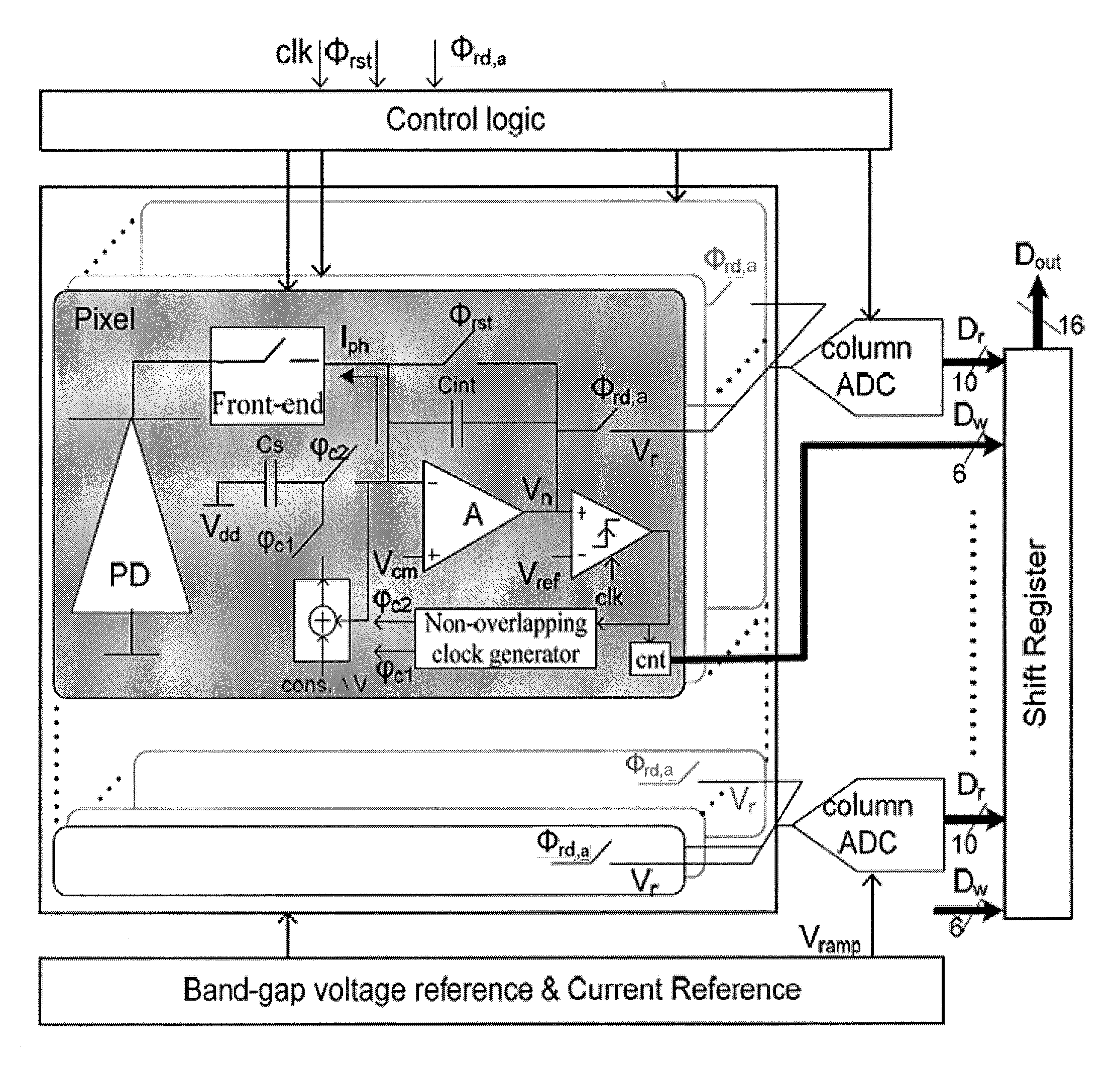
[0008]The invention provides a CMOS CT detector design with high linearity, quantum-limited noise, good scalability, high fill factor with a single CMOS chip utilizing synchronous partial quantization. In one embodiment, the CMOS CT detector includes: a pixel array including a plurality of pixels arranged into at least one column; at least one digital column bus corresponding to the at least one column; at least one analog column bus corresponding to the at least one column; at least one column processing circuit corresponding to the at least one column for processing digital and analog outputs received from the at least one digital column bus and the at least one analog column bus; a shift register for multiplexing outputs of at least two column processing circuits; a control signal generation circuit for generating controls signals for at least one of the plurality of pixels, the shift register, and the at least one column processing circuit; and a reference generation circuit for generating voltage and current references for at least one of the at least one column processing circuit and the plurality of pixels. In a synchronous partial quantization scheme, the pixel array operates in three exclusive clock phases including a reset phase, an integration phase and an analog readout phase corresponding to three control signals including a reset control signal, an integration control signal and an analog readout control signal.

Problems solved by technology

However, in this embodiment, the large capacitance of the photodiode (PD) 601 loads directly at the integration node 619, which increases the nonlinearity and noise of the pixel.
The capacitance at the integration node will cause extra charge loss from Cint if the offset varies.
However, the noise level of this work was slightly higher than the voltage-mode CT scanner described by L spies et al., which could be due to the addition of the current front-end.
While the current front-end increases the scanner linearity, it also increase the presence of noise.
However the noise level of the new scanner is still lower than the Poisson noise, which is sufficient for CT applications.

Method used


Image

  • Quantum-limited highly linear CMOS detector for computer tomography
  • Quantum-limited highly linear CMOS detector for computer tomography
  • Quantum-limited highly linear CMOS detector for computer tomography

Examples


Embodiment Construction

bodiment;

[0035]FIG. 20 is a simplified block diagram of a column circuit including a digital column bus and analog column bus in one embodiment;

[0036]FIG. 21 is a block diagram of a digital counter in one embodiment;

[0037]FIG. 22 is a timing diagram depicting the operation of control signals for the digital counter of FIG. 21 during Φint of one frame in one embodiment;

[0038]FIG. 23 is a micrograph of a prototype CMOS CT scanner with chip size 2 mm×2 mm according to one embodiment;

[0039]FIG. 24 is an oscilloscope screen depicting the outputs Vn and φc2 in an experiment involving the prototype depicted in FIG. 23;

[0040]FIG. 25 is a photograph depicting the electrical performance measurement set-up used to evaluate the performance of the prototype depicted in FIG. 23;

[0041]FIG. 26 is a graph showing noise and linearity measurements corresponding to the prototype depicted in FIG. 23; and

[0042]FIG. 27 is a graph showing an FFT analysis of measured data corresponding to the prototype depi...


PUM


Abstract

The invention provides a CMOS CT detector design with high linearity, quantum-limited noise, good scalability, high fill factor with a single CMOS chip utilizing synchronous partial quantization. The CMOS CT detector includes a pixel array, digital column buses, analog column buses, column processing circuits, a shift register, a control signal generation circuit, and a reference generation circuit, and implements a synchronous partial quantization scheme with reset, integration and analog readout phases. Each pixel of the pixel array further includes a photodiode; an integration capacitor; an OPAMP; a reset switch; a comparator; a 1-bit dynamic random-access-memory (DRAM) cell; a circuit block for enabling subtraction of a substantially fixed amount of charge from the integrated photocharge if the integrated photovoltage increases beyond the reference voltage; an integration node; an analog buffer; and a switch coupled between the output of the DRAM cell and the digital column bus. The inclusion of a level-shifter and a current front-end improves the linearity of the detector.

Description

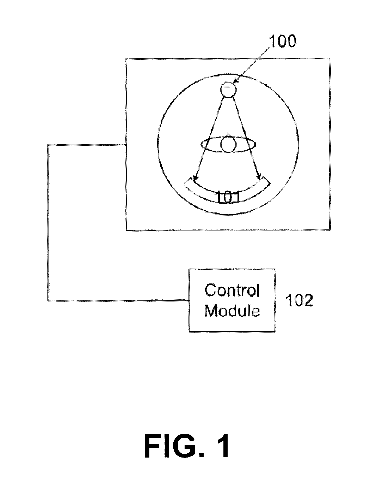
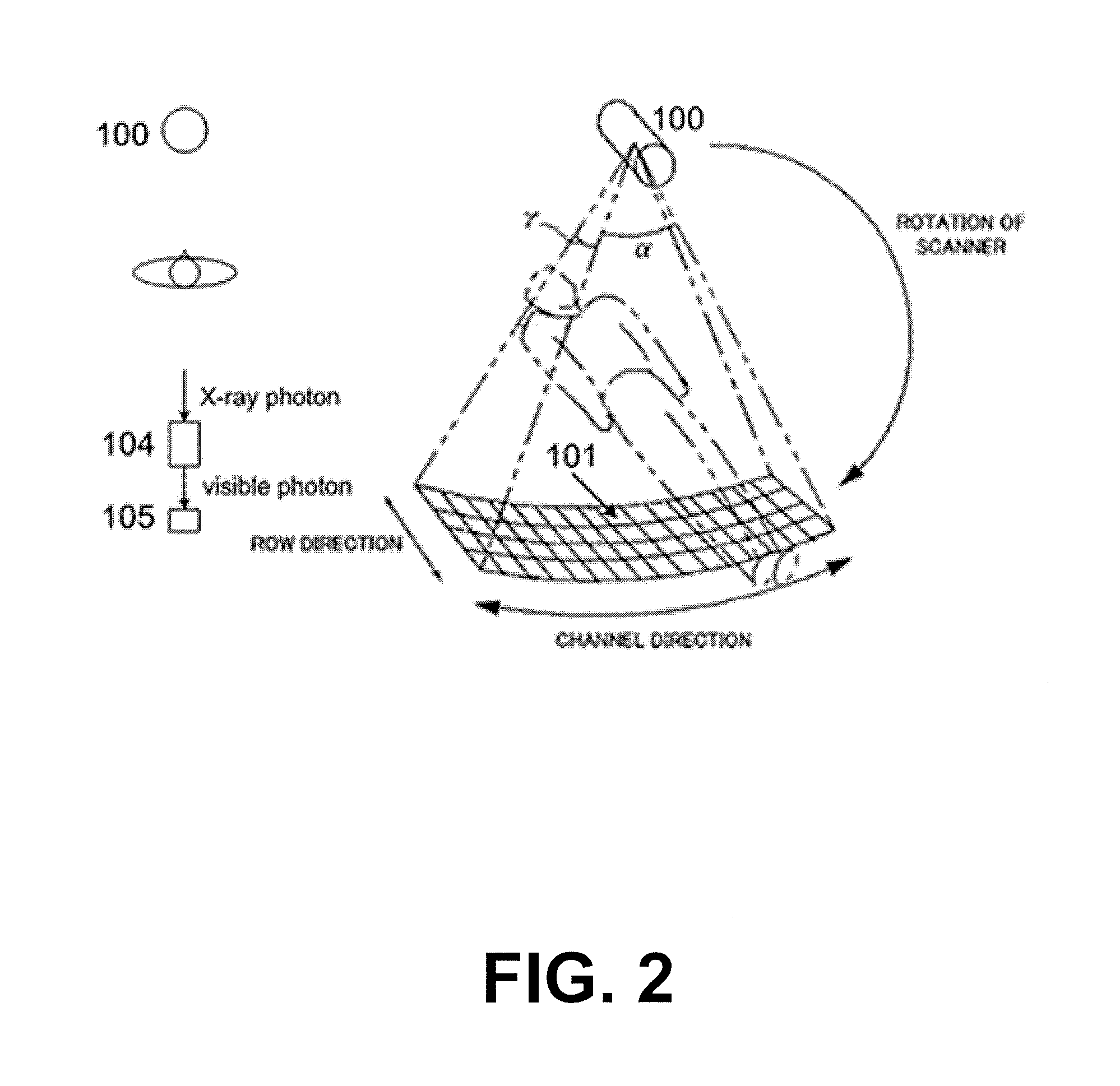
CROSS-REFERENCE TO RELATED APPLICATIONS[0001]This patent application claims the benefit of U.S. Provisional Patent Application No. 61 / 344,105, filed May 25, 2010, which is incorporated by reference.BACKGROUND OF THE INVENTION[0002]X-ray computed tomography (CT) is one of the major diagnostic imaging modalities. A multi-slice CT apparatus obtains projection data of an object by irradiating cone X-ray beams and measures the X-rays which have passed through the object by an X-ray detector. As shown in FIG. 1, an X-ray CT apparatus mainly includes an X-ray source 100, a 2-dimensional X-ray detector 101, and a control console 102. The projection data is acquired in discrete positions of the X-ray source in one rotation. The tomographic images of the object can be reconstructed by performing back projection on the projection data.[0003]X-ray CT detectors are mainly based on indirect conversion. FIG. 2 shows the impinging X-ray photons are converted into visible photons by a phosphor or sc...

Claims


Application Information

Patent Timeline
IPC IPC(8): G01T1/24
CPCG01T1/247G01T1/249H04N25/772
Inventor YUAN, JIELIU, BING
Owner THE HONG KONG UNIV OF SCI & TECH
Learn More