Crystal growth method and semiconductor device

a growth method and crystal technology, applied in semiconductor/solid-state device manufacturing, semiconductor devices, electrical equipment, etc., can solve the problems of reducing the production efficiency of gan, so as to reduce the production cost and reduce the production cost. , the effect of suppressing cracks

Active Publication Date: 2012-01-12
THE RITSUMEIKAN TRUST +1
View PDF4 Cites 10 Cited by
  • Summary
  • Abstract
  • Description
  • Claims
  • Application Information

AI Technical Summary

Benefits of technology

[0044]In the above-described semiconductor device according to the second aspect, the AlN layer containing the void may be removed eventually. In that case, it is preferable that the AlN layer containing the void be removed by dry etching such as RIE. Instead, it may be dissolved away chemically with a liquid such as hot phosphoric acid or molten KOH. While, as mentioned above, the AlN layer containing the void exerts an effect of mitigating strain and suppressing cracks when the device structure is grown on top of the substrate, it can also cause an increase in the driving voltage in a case where the substrate is removed before the device is completed. Thus, by removing the substrate and also the AlN layer, it is possible to reduce the driving voltage of the device and improve the wall-plug efficiency (the ratio of the light output to the electric power fed into the device; the higher the value, the lower the loss in the device and the higher the energy efficiency, which are preferable characteristics of the device).
[0045]As described above, according to the invention, it is possible to easily obtain a crystal growth method and a semiconductor device that help suppress development of dislocations and cracks, fabricated by that method.
[0046]Moreover, according to the invention, it is possible to easily obtain a crystal growth method that helps suppress a warp in a substrate.
[0047]Furthermore, according to the invention, it is possible to easily obtain a crystal growth method and a semiconductor device that help reduce costs.

Problems solved by technology

On the other hand, with GaN-based compound semiconductors, bulk crystal growth is difficult, and this makes practically usable GaN substrates extremely expensive.
Inconveniently, however, even that method is ineffective in coping with lattice mismatch between substrate and crystal, with the result that the grown GaN has numberless defects.
These defects will probably prove a hindrance in the fabrication of GaN-based LDs (laser diodes).
Inconveniently, however, with the conventional methods mentioned above, in high-Al-content AlGaN ternary alloy growth which is required for the formation of ultraviolet light-emitting devices, the large differences in lattice constant and in thermal expansion coefficient between substrate and epitaxial layer tend to cause development of cracks or a warp in the substrate.
Cracks disrupt the device structure, leading to unsatisfactory characteristics, and reduces the number of acceptable devices obtained from a single wafer, leading to diminished yields.
On the other hand, a warp in the substrate not only makes the substrate prone to break during handling, but also makes it difficult, when forming a mask pattern on the substrate in a photolithography step or the like in the device process, to achieve uniform focus across the substrate surface, leading to diminished yields in device fabrication.

Method used


Image

  • Crystal growth method and semiconductor device
  • Crystal growth method and semiconductor device
  • Crystal growth method and semiconductor device

Examples


embodiment 1

[0068]As discussed earlier, crystal growth of a group III nitride semiconductor is liable to encounter development of cracks or a warp in the substrate. In particular, in the fabrication of ultraviolet light-emitting devices that emit light in an ultraviolet region, a nitride semiconductor layer with a high Al content needs to be formed with a comparatively large thickness, and this makes development of dislocations and cracks, and of a warp in the substrate, extremely likely.

[0069]Through intensive studies in search of a solution to the above problem, the present inventors have found that, when a material that reacts with a substrate is fed onto the substrate before crystal growth, a depressed structure forms spontaneously on the substrate surface. The inventors have further found that, by forming a nitride semiconductor layer on top of a substrate having such a depressed structure formed on it, it is possible to form a high-Al-content nitride semiconductor layer that is crack-free...

embodiment 2

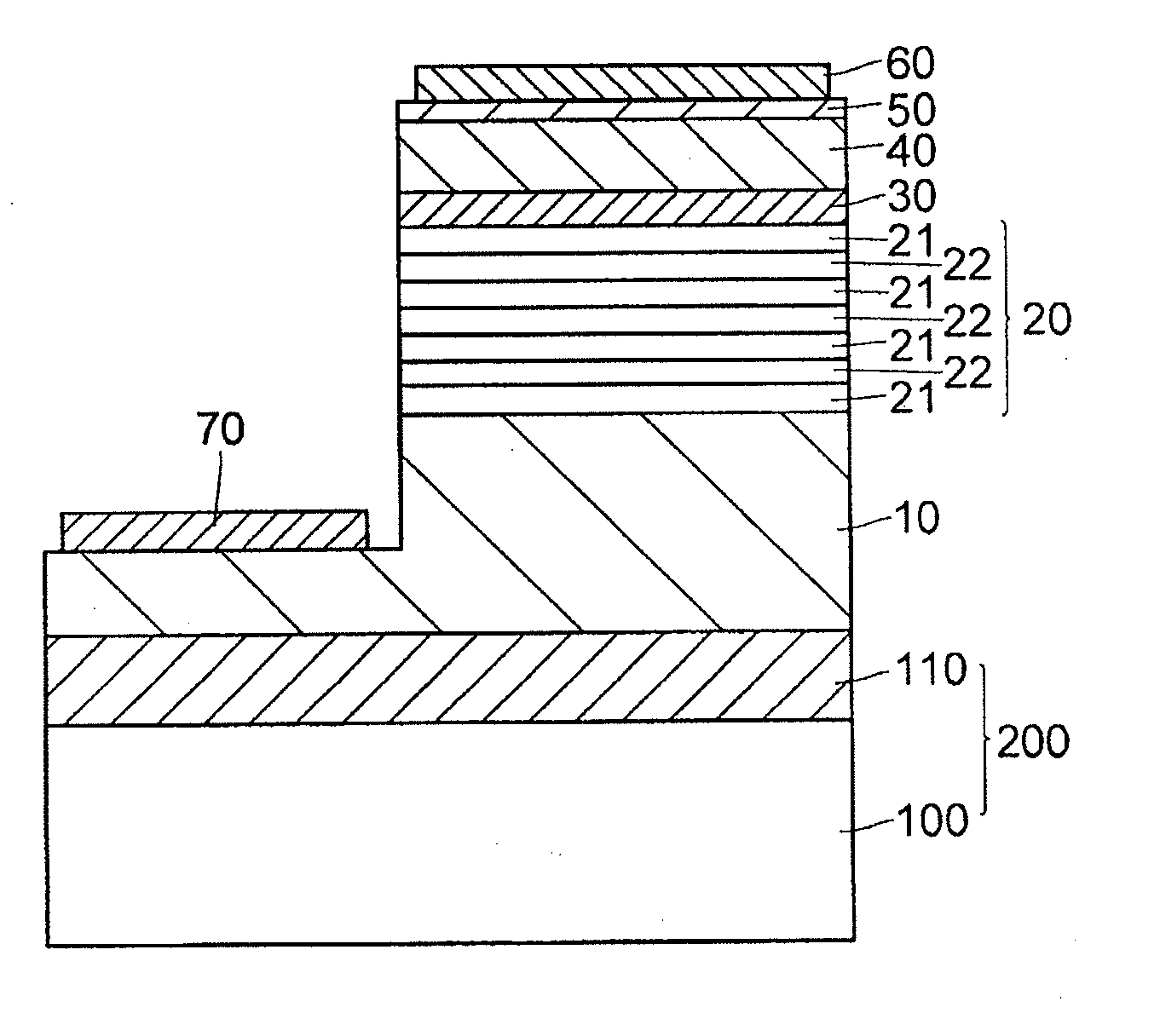
[0124]FIG. 10 is a sectional view of a light-emitting diode device according to a second embodiment (Embodiment 2) of the invention. Next, with reference to FIGS. 1 and 10, the light-emitting diode device (semiconductor device) according to Embodiment 2 of the invention will be described.

[0125]The light-emitting diode device according to Embodiment 2 is an ultraviolet light-emitting device that emits light in an ultraviolet region, and more particularly a far-ultraviolet light-emitting device that emits light in a far-ultraviolet region of 200 nm to 350 nm. This light-emitting diode device is provided with a template substrate 200 which has an AlN buffer layer 110 formed on top of a silicon substrate 100, and has a plurality of nitride semiconductor layers stacked on top of the template substrate 200. In the light-emitting diode device according to Embodiment 2, formed on top of the AlN buffer layer 110 of the template substrate 200 are high-Al-content nitride semiconductor layers.

[...

embodiment 3

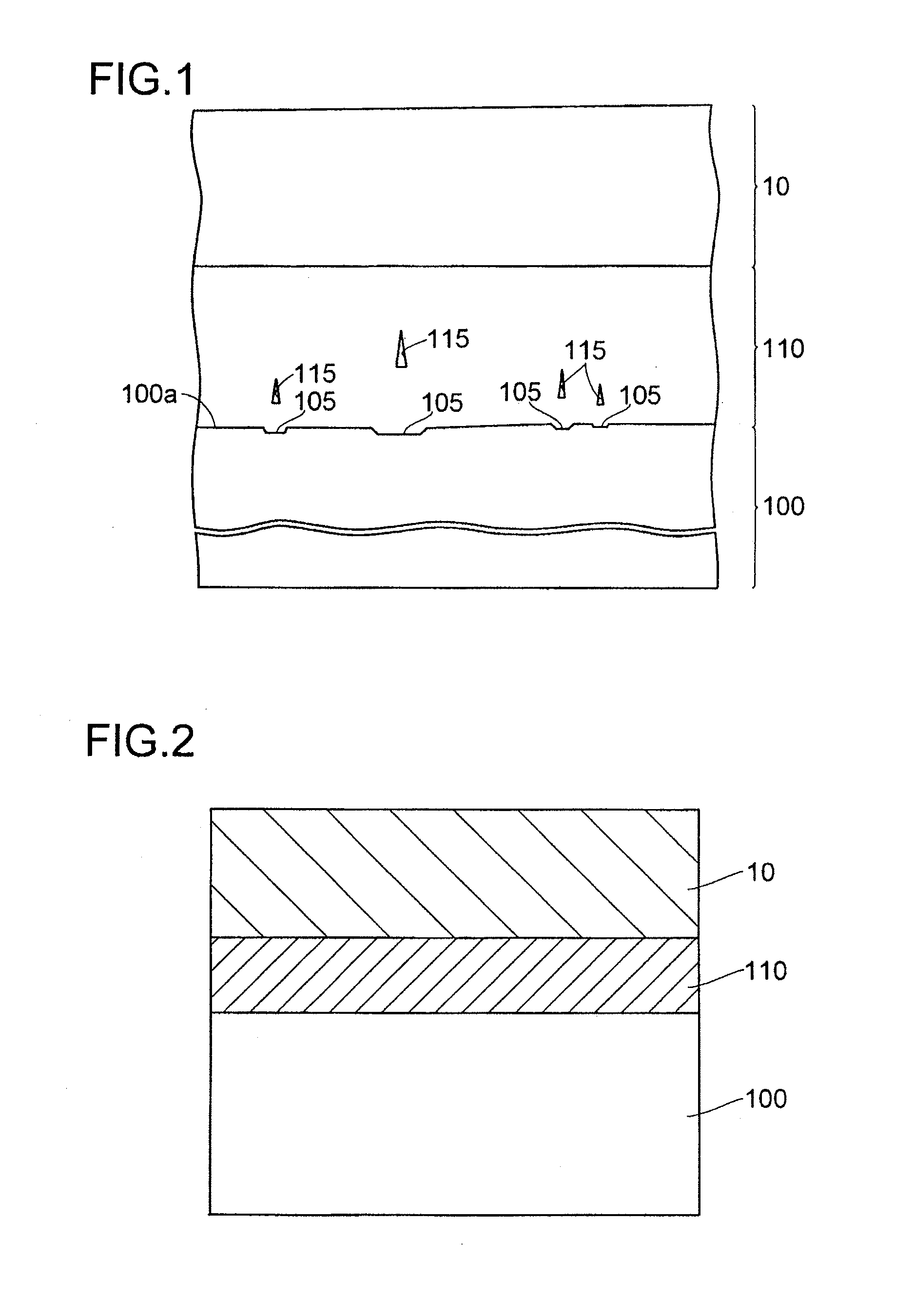
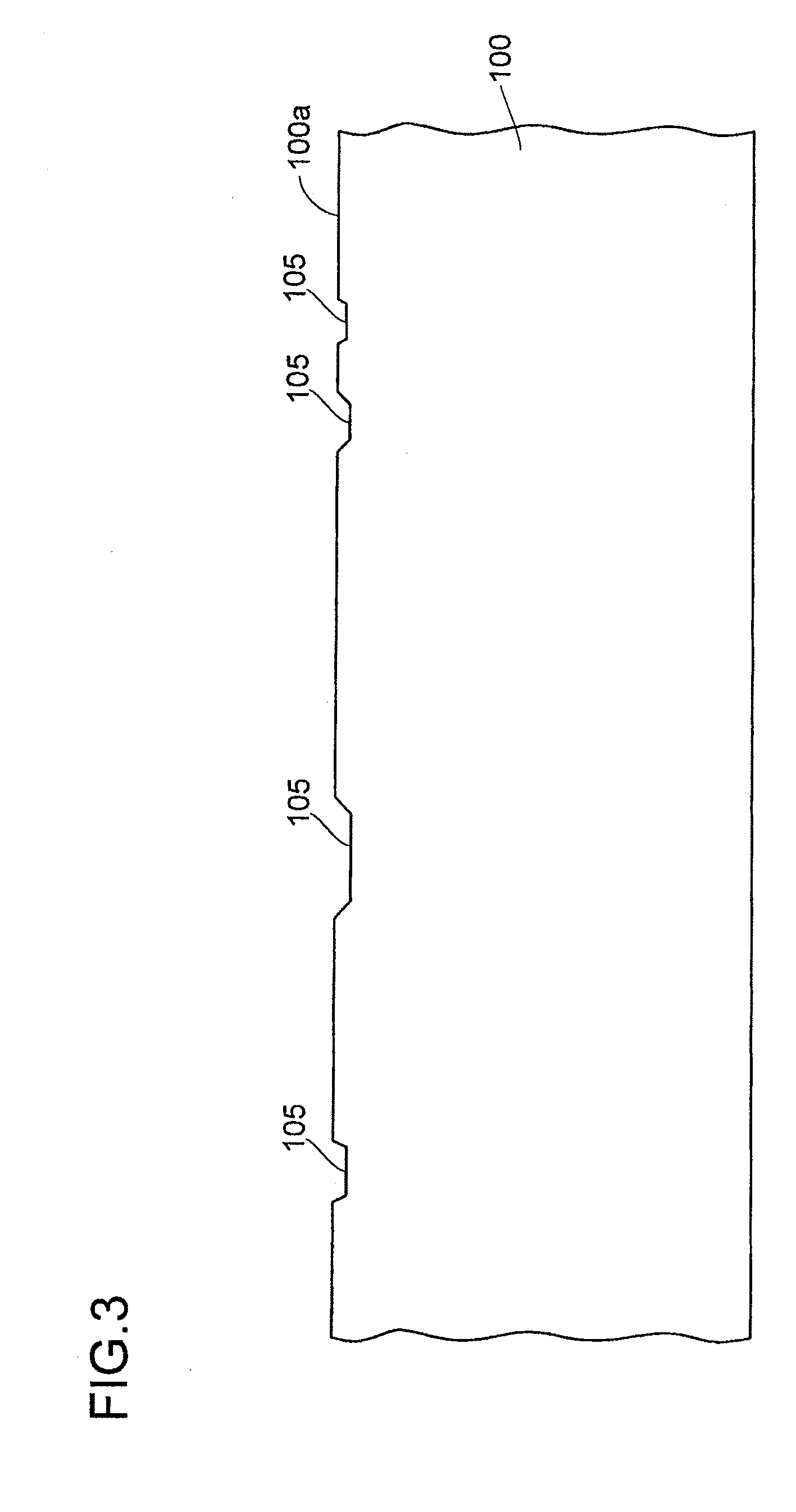
[0143]FIG. 12 is a sectional view of a light-emitting diode device according to a third embodiment (Embodiment 3) of the invention. Now, with reference to FIG. 12, the light-emitting diode device (semiconductor device) according to Embodiment 3 of the invention will be described. In FIGS. 10 and 12, corresponding parts are identified by the same reference signs, and no overlapping description will be repeated unless necessary.

[0144]In the light-emitting diode device according to Embodiment 3, the structure differs from that of Embodiment 2 described previously in that the silicon substrate 100 (see FIG. 10) is removed by chemical processing using a chemical liquid or the like. Then, on the back surface of the AlN buffer layer exposed as a result of removal of the silicon substrate 100, the n-side electrode 70 is formed. The n-side electrode 70 is, for example, a Ni / Au electrode of a multiple layer structure having a Ni layer (not shown) and a Au layer (not shown) stacked in this ord...


PUM

PropertyMeasurementUnit
temperatureaaaaaaaaaa
thicknessaaaaaaaaaa
thicknessaaaaaaaaaa

Abstract

A method of crystal growth is provided which can suppress development of dislocations and cracks and a warp in a substrate. The method of crystal growth of a group III nitride semiconductor has: a step of heating a silicon substrate; and a step of forming a depressed structure on the substrate surface by advance-feeding onto the heated silicon substrate a gas containing at least TMA (trimethylaluminum).

Description

[0001]This nonprovisional application claims priority under 35 U.S.C. §119(a) on Patent Application No. 2010-155388 filed in Japan on Jul. 8, 2010 and Patent Application No. 2011-042479 filed in Japan on Feb. 28, 2011, the entire contents of both of which are hereby incorporated by reference.BACKGROUND OF THE INVENTION[0002]1. Field of the Invention[0003]The present invention relates to a crystal growth method and a semiconductor device, and more particularly to a crystal growth method for a nitride-based compound semiconductor and a semiconductor device formed thereby.[0004]2. Description of Related Art[0005]GaN-based compound semiconductors such as GaN, InGaN, and AlGaN are receiving attention as materials for blue light-emitting diodes (LEDs) and laser diodes (LDs). For their good thermal and environmental resistance, GaN-based compound semiconductors are today applied in and developed for electronic devices as well.[0006]On the other hand, with GaN-based compound semiconductors,...

Claims


Application Information

Patent Timeline
Patent Type & Authority Applications(United States)
IPC IPC(8): H01L33/04H01L21/20
CPCH01L21/0237H01L21/02381H01L21/0243H01L21/02458H01L33/007H01L21/0262H01L21/02639H01L21/02658H01L21/0254
Inventor UETA, YOSHIHIROOHTA, MASATAKAAOYAGI, YOSHINOBUTAKEUCHI, MISAICHI
Owner THE RITSUMEIKAN TRUST
Why Eureka
Try Eureka