

Transparent conductive film and method for manufacturing transparent conductive film
a technology manufacturing method, which is applied in the field of transparent conductive film, can solve the problems of inapplicability to the device application required, inferior manufacturing efficiency, and high manufacturing cost, and achieve excellent surface conductivity, high optical transmittance, and low cost
- Summary
- Abstract
- Description
- Claims
- Application Information
AI Technical Summary
Benefits of technology
Problems solved by technology
Method used
Image

Examples
example 1
Preparation of Transparent Conductive Film
[0110]Preparation of Transparent conductive film TC-1A
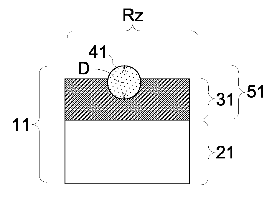
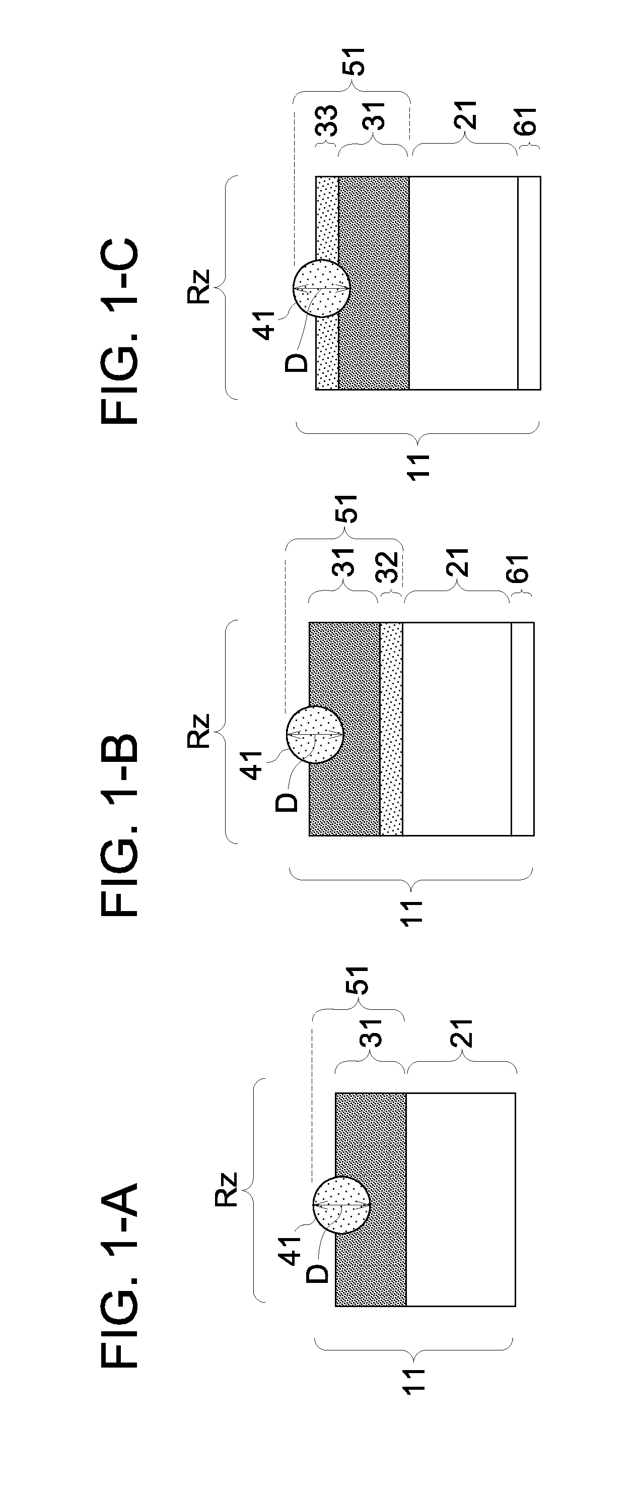
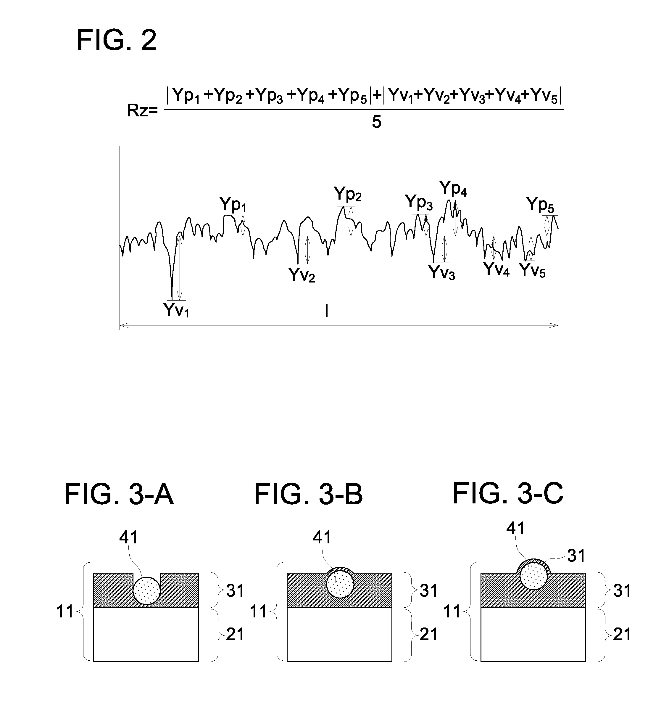
[0111]A transparent electrode was produced according to the preferable manufacturing process of the transparent conductive film of the present invention shown in the above-mentioned FIG. 4. As a mold-releasing substrate, it was used a PET film having a clear hard coat layer (CHC) as a mold releasing surface, having the surface smoothness of Rz=9 nm and Ra=1 nm.
(1) After applying a silver nanowire dispersion liquid to the mold-releasing substrate which had been performed corona discharge treatment so that the coverage of silver nanowire may be set to 60 mg / m2, the dry process was carried out at 120° C. for 30 minutes, and a silver nanowire network structure was formed.
(2) Subsequently, an aqueous solution of polyvinyl alcohol (PVA) as a soluble binder overcoat was overcoated to the above-mentioned silver nanowire network structure so that the dried thickness might be set to 5 nm. In additi...
example 2
Evaluation of Transparent Conductive Film
(Evaluation of Exposure of Conductive Fibers)
[0125]Etching treatment was carried out to the transparent conductive films TC-1A to TC-1M prepared in Examples 1. Exposure of conductive fibers was evaluated by measuring the change of the surface resistivity before and after the etching treatment. The etching treatment was performed by immersing each transparent conductive film in an etching solution having the following composition for 1 minute. Each transparent conductive film after being carried out the etching treatment was subjected to washing treatment with running water, then it was fully dried.
(Etching Solution)
[0126]
Ethylenediaminetetraacetic acid iron (III) ammonium salt60 gEthylenediaminetetraacetic acid 2 gSodium metabisulfite15 gAmmonium thiosulfate70 gMaleic acid 5 g
[0127]Adding pure water to become 1 L, and then adjusted to pH 5.5 with sulfuric acid, or an aqueous ammonia solution.
[0128]When surface resistivity before an etching pr...
PUM
| Property | Measurement | Unit |
|---|---|---|
| total optical transmittance | aaaaa | aaaaa |
| optical transmittance | aaaaa | aaaaa |
| optical transmittance | aaaaa | aaaaa |
Abstract
Description
Claims
Application Information