
Simulated wirebond semiconductor package

a semiconductor and wire bond technology, applied in the direction of non-electric welding apparatus, manufacturing tools, solventing apparatus, etc., can solve the problems of device not being connected to the final pcb, size and distance between die terminals being so small, and achieve high-performance effects

Inactive Publication Date: 2012-03-15
HSIO TECH
View PDF9 Cites 69 Cited by
  • Summary
  • Abstract
  • Description
  • Claims
  • Application Information

AI Technical Summary

Benefits of technology

[0009]The present disclosure relates to the use of additive printing processes to create polymer-based metallic contacts that replace conventional wirebonds with simulated wirebonds to provide a low-cost, high-performance package. The printing process provides unique opportunity to add function or performance enhancement within the package structure not seen in traditional packages. The present semiconductor package can be used with single or multiple IC devices.
[0011]The use of additive printing processes permits the material set in a given layer to vary. Traditional PCB and flex circuit fabrication methods take sheets of material and stack them up, laminate, and / or drill. The materials in each layer are limited to the materials in a particular sheet. Additive printing technologies permit a wide variety of materials to be applied on a layer with registration relative to the features of the previous layer. Selective addition of conductive, non-conductive, or semi-conductive materials at precise locations to create a desired effect has the major advantages in tuning impedance or adding electrical function on a given layer. Tuning performance on a layer by layer basis relative to the previous layer greatly enhances electrical performance.
[0020]The present disclosure is also directed to several additive processes that combine the mechanical or structural properties of a polymer material, while adding metal materials in an unconventional fashion, to create electrical paths that are refined to provide electrical performance improvements. By adding or arranging metallic particles, conductive inks, plating, or portions of traditional alloys, the compliant printed semiconductor package reduces parasitic electrical effects and impedance mismatch, potentially increasing the current carrying capacity.
[0022]The semiconductor package can be configured with conductive traces that reduce or redistribute the terminal pitch, without the addition of an interposer or daughter substrate. Grounding schemes, shielding, electrical devices, and power planes can be added to the semiconductor package, reducing the number of connections to the PCB and relieving routing constraints while increasing performance.

Problems solved by technology

In many cases, the size and distance between die terminals is so small that the device cannot be connected to the final PCB without some sort of fan out or routing.
In many cases, the size and distance between die terminals is so small that the IC device cannot be connected to the final PCB without some sort of re-routing interface.
In most cases, the connection of the IC device to the package is generally not reworkable once packaged and if there is a missing or broken connection it is difficult to repair.
Both methods have benefits and limitations.
The leads and wirebonds also have a relatively high inductance which can degrade electrical performance.
One limitation of the no lead types of packages is the lack of compliance at the terminal when soldered to the PCB.
The solder reflowed to join the pad on the package to the pad on the PCB can see significant stress during thermal cycling or physical shock such as dropping a cell phone.
Placing multiple IC devices in a single package further complicates the problems discussed above.

Method used


Image

  • Simulated wirebond semiconductor package
  • Simulated wirebond semiconductor package
  • Simulated wirebond semiconductor package

Examples


Embodiment Construction

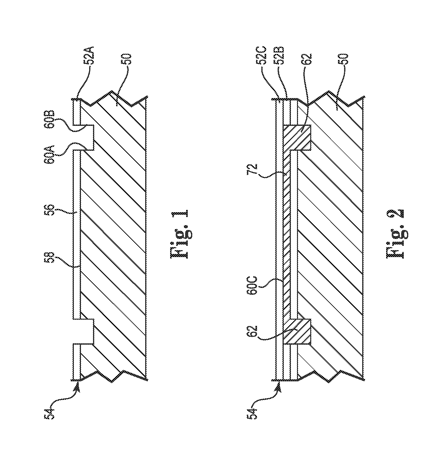
[0040]FIG. 1 is a side sectional view of substrate 50 with first layer 52A of a simulated wirebonds 54 for making a semiconductor package in accordance with an embodiment of the present disclosure. In the illustrated embodiment, the substrate 50 optionally includes pre-formed recesses 60A. The first layer 52A is preferably a dielectric material 56 selectively printed on surface 58 of the substrate 50 around recesses 60A.

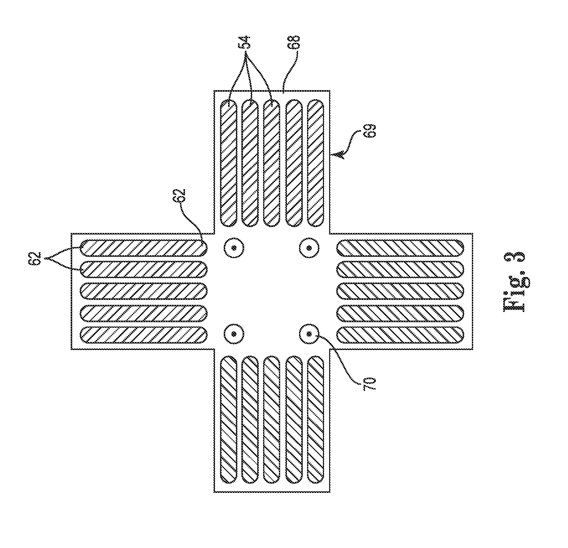
[0041]As best illustrated in FIG. 2, recesses 60B in the dielectric material 56 and the recesses 60A are then metalized to create contact pads 62. Metalizing can be performed by printing conductive particles followed by a sintering step, by printing conductive inks, or a variety of other techniques. The metalizing material is preferably of copper or similar metallic materials such as phosphor bronze or beryllium-copper. The resulting contact pads 62 are optionally plated to improve conductive properties. The plating is preferably a corrosion resistant metallic materi...


PUM

PropertyMeasurementUnit
Dielectric polarization enthalpyaaaaaaaaaa
Shapeaaaaaaaaaa
Electrical conductoraaaaaaaaaa

Abstract

A semiconductor package with simulated wirebonds. A substrate is provided with a plurality of first pads on a first surface and a plurality of second pads on a second surface. Each of the first pads are electrically coupled to one or more of the second pads. At least one semiconductor device is located proximate the first surface of a substrate. The simulated wirebonds include at least a first dielectric layer selectively printed to create a plurality of recesses, and a conductive material located in the recesses to form first and second contact pads, and electrical traces electrically coupling the first and second contact pads. The first contact pads are electrically coupled to terminals on the semiconductor device and the second contact pads are electrically coupled to the first pads on the first surface of the substrate. An overmolding material seals the semiconductor device and the simulated wirebonds

Description

TECHNICAL FIELD[0001]The present disclosure leverages the capabilities of the additive printing process to create a high performance electrical interconnect between integrated circuits and semiconductor packages. The printing process provides unique opportunity to add function or performance enhancement within the package structure not seen in traditional packages.BACKGROUND OF THE INVENTION[0002]Traditional semiconductors and IC devices are typically packaged in a variety of ways to provide redistribution from the terminals on the die to a spacing that is conducive to cost effective printed circuit board (“PCB”) fabrication techniques. In many cases, the size and distance between die terminals is so small that the device cannot be connected to the final PCB without some sort of fan out or routing. The packages also serve to protect the fragile silicon or provide additional functions such as thermal management or near device decoupling. In many cases, the size and distance between d...

Claims


Application Information

Patent Timeline
IPC IPC(8): H01L23/48H01L21/56
CPCB23K1/0016B23K20/004H01L2924/1306B23K2201/42H01L21/6835H01L23/3107H01L23/48H01L23/552H01L24/50H01L24/86H01L25/0655H01L25/0657H01L2223/6677H01L2924/01004H01L2924/01013H01L2924/01015H01L2924/01029H01L2924/01046H01L2924/01049H01L2924/01075H01L2924/01078H01L2924/01079H01L2924/01082H01L2924/09701H01L2924/12044H01L2924/14H01L2924/19041H01L2924/19042H01L2924/19043H01L2924/30107H01L2924/3011H01L2924/3025H01L2924/01005H01L2924/01006H01L2924/01033H01L2924/01047H01L2924/014H01L2225/06524H01L2225/06568H01L2924/00B23K2101/42H01L2924/181H01L2924/00012
Inventor RATHBURN, JAMES
Owner HSIO TECH
Features
  • Generate Ideas
  • Intellectual Property
  • Life Sciences
  • Materials
  • Tech Scout
  • Unparalleled Data Quality
  • Higher Quality Content
  • 60% Fewer Hallucinations
Learn More