Multilayered material and method of producing the same

a technology of multi-layered materials and layered materials, applied in the field of multi-layered materials, can solve the problems of poor abrasion resistance of inorganic polymer layers, inability to prevent deterioration of substrates, and inability to achieve good abrasion resistance, so as to reduce the influence of optical precision, improve the efficiency of optical components, and improve the effect of refractive index controllability

Inactive Publication Date: 2012-05-03
MITSUI CHEM INC
View PDF7 Cites 405 Cited by
  • Summary
  • Abstract
  • Description
  • Claims
  • Application Information

AI Technical Summary

Benefits of technology

[0066]Since the method of producing a multilayered material according to the present invention can reduce an influence on precision of an optical member, it is possible to produce a multilayered materia...

Problems solved by technology

However, this method has a problem that it takes much time to form silica and a problem that the substrate can not be prevented deterioration by exposing to a high temperature.
As described in an example of Patent Document 1, in a technique generally called a corona process using air as a plasma species, the obtained inorganic polymer layer does not exhibit a satisfactory gas barrier property.
There is also a problem in that abrasion resistance thereof is not good.
The gas barrier property required in uses such as members of an FPD or solar cells and flexible substrates and sealing films of organic EL devices is a level which is difficult to realize in a silicon oxide (silica) single film.
Accordingly, the gas-barrier films described in Patent Document 1 and Patent Document 2 still have problems to be so...

Method used


Image

  • Multilayered material and method of producing the same
  • Multilayered material and method of producing the same
  • Multilayered material and method of producing the same

Examples


example 1

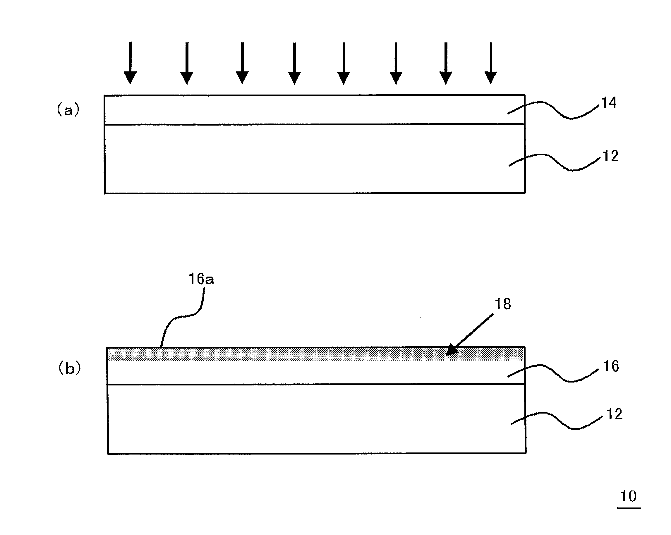
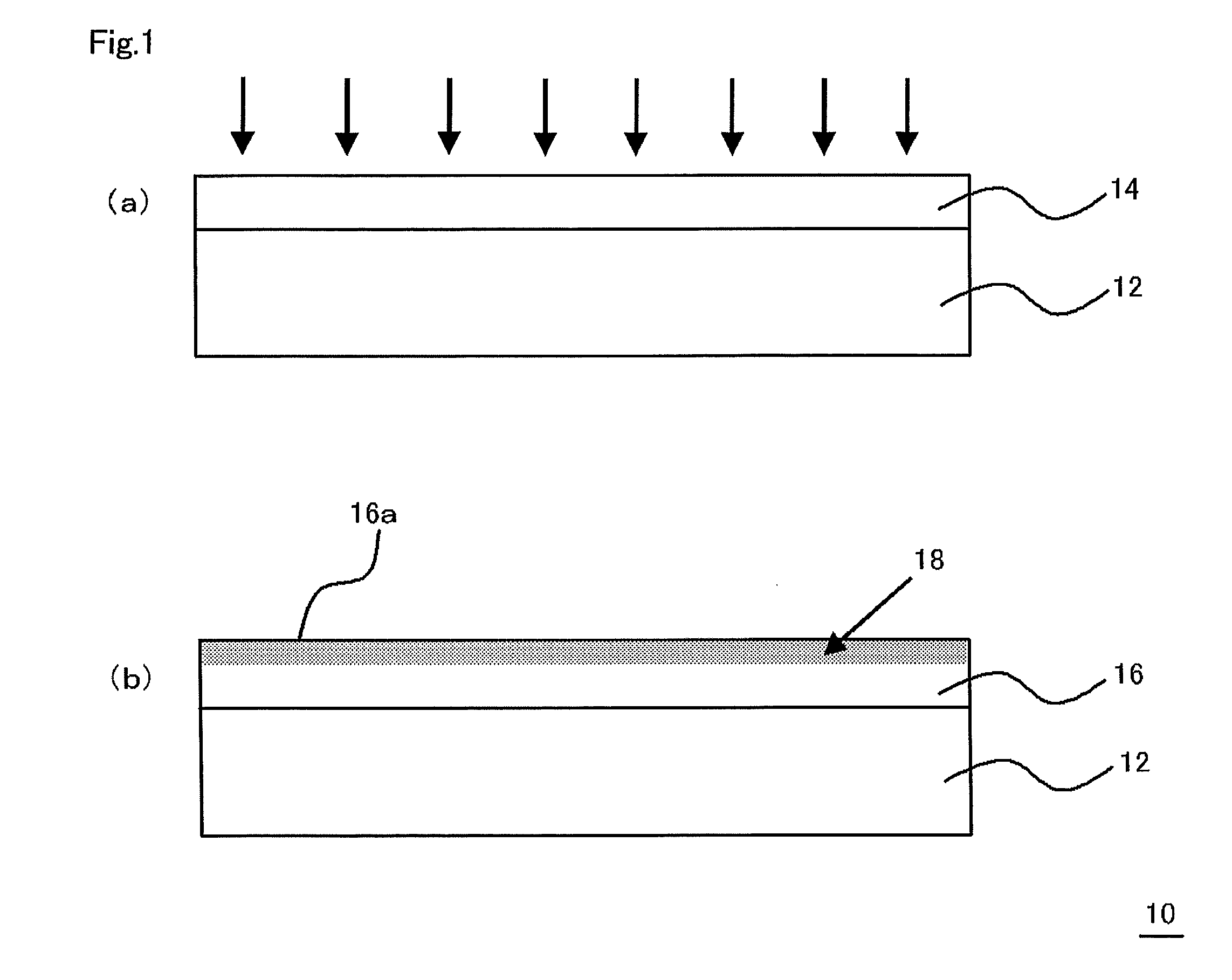
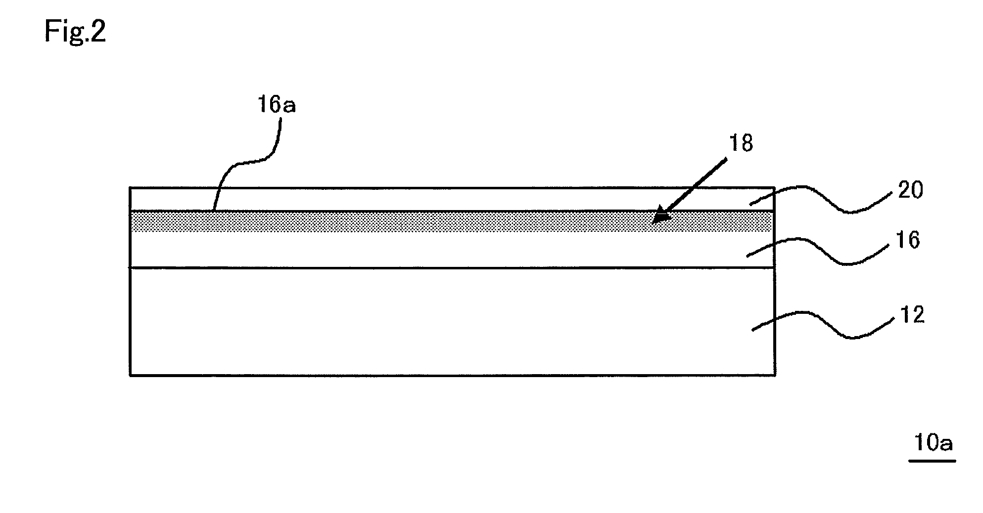
[0173]A silicon substrate (with a thickness of 530 μm, made by Shin-Etsu Chemical Co., Ltd.) was spin-coated (at 3000 rpm for 10 s) with a 2 wt % xylene (dehydrated) solution of polysilazane (NL110A made by AZ Electronic Materials S.A.), and then the resultant was dried at 120° C. for 10 minutes under the nitrogen atmosphere, whereby a polysilazane film with a thickness of 0.025 μm was produced. The drying was performed under an atmosphere in which the water vapor concentration is about 500 ppm.

[0174]A vacuum plasma process was performed on the polysilazane film under the following conditions.[0175]Vacuum plasma processing apparatus: made by U-TEC Corporation[0176]Gas: Ar[0177]Gas flow rate: 50 mL / min[0178]Pressure: 19 Pa[0179]Temperature: room temperature[0180]Power applied per unit area of electrode: 1.3 W / cm2 [0181]Frequency: 13.56 MHz[0182]Process time: 5 min

example 2

[0183]A silicon substrate (with a thickness of 530 μm, made by Shin-Etsu Chemical Co., Ltd.) was spin-coated (at 3000 rpm for 10 s) with a 2 wt % xylene (dehydrated) solution of polysilazane (NL110A made by AZ Electronic Materials S.A.) to which a catalyst was not added, and then the resultant was dried under the same conditions as Example 1, whereby a polysilazane film with a thickness of 0.025 μm was produced.

[0184]Subsequently, a vacuum plasma process was performed under the same conditions as Example 1.

example 3

[0185]A polyethylene terephthalate (PET) film (with a thickness of 50 μm, “A4100” made by Toyobo Co., Ltd.) was bar-coated with a 2 wt % xylene (dehydrated) solution of polysilazane (NL110A made by AZ Electronic Materials S.A.), and then the resultant was dried under the same conditions as Example 1, whereby a polysilazane film with a thickness of 0.1 μm was produced.

[0186]Subsequently, a vacuum plasma process was performed under the same conditions as Example 1.


PUM

PropertyMeasurementUnit
Thicknessaaaaaaaaaa
Thicknessaaaaaaaaaa
Thicknessaaaaaaaaaa

Abstract

A multilayered material is provided which includes a substrate and a silicon-containing film formed on the substrate, wherein the silicon-containing film has a nitrogen-rich area including silicon atoms and nitrogen atoms, or silicon atoms, nitrogen atoms, and an oxygen atoms and the nitrogen-rich area is formed by irradiating a polysilazane film formed on the substrate with an energy beam in an atmosphere not substantially including oxygen or water vapor and denaturing at least a part of the polysilazane film. A method of producing the multilayered material is also provided.

Description

TECHNICAL FIELD[0001]The present invention relates to a multilayered material and a production method thereof.BACKGROUND ART[0002]Recently, for blocking gases such as oxygen or water vapor, transparent gas-barrier materials become to be used in members (such as substrates and back sheets) of flat panel displays (FPD) such as liquid crystal displays or solar cells, flexible substrates or sealing films of organic electroluminescence (organic EL) devices, and the like, in addition to traditional main use such as packaging materials of food and medicines. Such applications require a very high gas barrier property.[0003]The transparent gas-barrier materials currently employed in some uses are produced by a dry method such as a plasma CVD method, a sputtering method, an ion plating method and a wet method such as a sol-gel method. Both methods are techniques of depositing silicon oxide (silica) exhibiting a gas barrier property on a plastic substrate. Since the wet method does not require...

Claims


Application Information

Patent Timeline
IPC IPC(8): B32B3/00C08J7/18B32B9/04B29C71/04C09D183/16C01B21/087C08J7/043C08J7/046C08J7/048
CPCC08J7/047C08J2483/16C09D183/16C08G77/62Y10T428/265C08J7/0427C08J7/048C08J7/043C08J7/046B32B27/08B32B27/16B32B9/00G02B1/10
Inventor TAKAKI, TOSHIHIKOFUKUMOTO, HARUHIKO
Owner MITSUI CHEM INC
Why Eureka
Try Eureka